

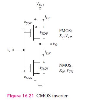
For the CMOS inverter in Figure 16.21, let (V_{D D}=3.3 mathrm{~V}, k_{n}^{prime}=100 mu mathrm{A} / mathrm{V}^{2}), (k_{p}^{prime}=40
Question:
For the CMOS inverter in Figure 16.21, let \(V_{D D}=3.3 \mathrm{~V}, k_{n}^{\prime}=100 \mu \mathrm{A} / \mathrm{V}^{2}\), \(k_{p}^{\prime}=40 \mu \mathrm{A} / \mathrm{V}^{2}, V_{T N}=0.4 \mathrm{~V}\), and \(V_{T P}=-0.4 \mathrm{~V}\).
(a) Let \((W / L)_{n}=2\) and \((W / L)_{p}=5\). (i) Find the transition points for the p-channel and \(n\)-channel transistors. (ii) Sketch the voltage transfer characteristics including the appropriate voltage values at the transition points. (iii) Find \(v_{I}\) for \(v_{O}=0.25 \mathrm{~V}\) and \(v_{O}=3.05 \mathrm{~V}\).
(b) Repeat part (a) for \((W / L)_{n}=4\) and \((W / L)_{p}=5\).
Step by Step Answer:

This question has not been answered yet.
You can Ask your question!
Related Book For 

Microelectronics Circuit Analysis And Design
ISBN: 9780071289474
4th Edition
Authors: Donald A. Neamen
Question Posted:
