

(a) Redesign the circuit shown in Figure P5.49 using (V_{C C}=9 mathrm{~V}) such that the voltage drop...
Question:
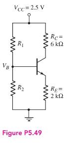
(a) Redesign the circuit shown in Figure P5.49 using \(V_{C C}=9 \mathrm{~V}\) such that the voltage drop across \(R_{C}\) is \(\left(\frac{1}{3}\right) V_{C C}\) and the voltage drop across \(R_{E}\) is \(\left(\frac{1}{3}\right) V_{C C}\). Assume \(\beta=100\). The quiescent collector current is to be \(I_{C Q}=\) \(0.4 \mathrm{~mA}\), and the current through \(R_{1}\) and \(R_{2}\) should be approximately \(0.2 I_{C Q}\).
(b) Replace each resistor in part (a) with the closest standard value (Appendix C). What is the value of \(I_{C Q}\) and what are the voltage drops across \(R_{C}\) and \(R_{E}\) ?
Fantastic news! We've Found the answer you've been seeking!
Step by Step Answer:

Answered By
Vikash Gupta
I am graduated in Physics in 2018, from KIRORIMAL COLLEGE, University of Delhi. Now I am persuing Master's degree in physics. I like to do physics problems. I have experience of 1 year in tutoring. I think Physics is the only subject where you understand things,how they are happening . In physics you learn Maths and apply it. So I would like to join your platform to solve many Physics problems.
5+ Reviews
10+ Question Solved
Related Book For 

Microelectronics Circuit Analysis And Design
ISBN: 9780071289474
4th Edition
Authors: Donald A. Neamen
Question Posted:
