

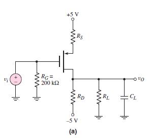
In the common-source amplifier in Figure 7.25 (a) in the text, a source bypass capacitor is to
Question:
In the common-source amplifier in Figure 7.25
(a) in the text, a source bypass capacitor is to be added between the source terminal and ground potential. The circuit parameters are \(R_{S}=3.2 \mathrm{k} \Omega, R_{D}=10 \mathrm{k} \Omega, R_{L}=20 \mathrm{k} \Omega\), and \(C_{L}=10 \mathrm{pF}\). The transistor parameters are \(V_{T P}=-2 \mathrm{~V}, K_{P}=0.25 \mathrm{~mA} / \mathrm{V}^{2}\), and \(\lambda=0\).
(a) Derive the small-signal voltage gain expression, as a function of \(s\), that describes the circuit behavior in the high-frequency range.
(b) What is the expression for the time constant associated with the upper \(3 \mathrm{~dB}\) frequency?
(c) Determine the time constant, upper \(3 \mathrm{~dB}\) frequency, and small-signal midband voltage gain.
Figure 7.25(a):-
Step by Step Answer:


Microelectronics Circuit Analysis And Design
ISBN: 9780071289474
4th Edition
Authors: Donald A. Neamen
