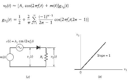
Figure a show the circuit diagram of a switching modulator. Assume that the carrier wave c (t)
Question:
Figure a show the circuit diagram of a switching modulator. Assume that the carrier wave c (t) applied to the diode is large in amplitude, so that the diode acts like an ideal switch: it presents zero impedance when forward biased (i.e. c (t) > 0). We may thus approximate the transfer characteristics of the diode-load resistor combination by piece-wise-linear characteristics defined as (see Figure b). That is, the load voltage v2 (t) varies periodically between the values v1 (t) and zero at a rate equal to the carrier frequency ??c. Hence, we may write, where gT0 (t) is a periodic pulse train defined by
(a) Find the AM wave component contained in the output voltage v2 (t).
(b) Specify the unwanted components in v2 (t) that need to be removed by a band-pass filter of suitabledesign.

Step by Step Answer:


