

Question: Design a CMOS op amp based on the folded-cascode architecture of Fig. 6.28 using supply voltages of ± 1.5 V. Use the bias circuit of
Design a CMOS op amp based on the folded-cascode architecture of Fig. 6.28 using supply voltages of ± 1.5 V. Use the bias circuit of Fig. 4.42 (with M3and M4cascoded) to generate the bias current IBIAS. Then design an extension to this bias circuit that
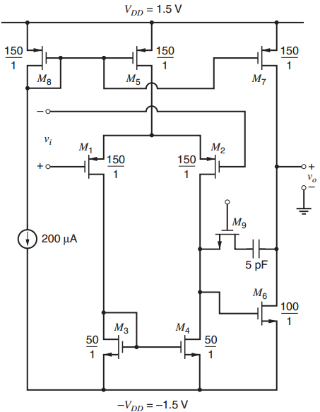
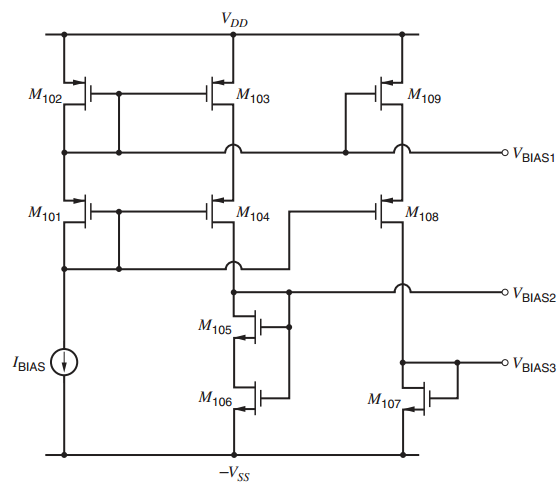
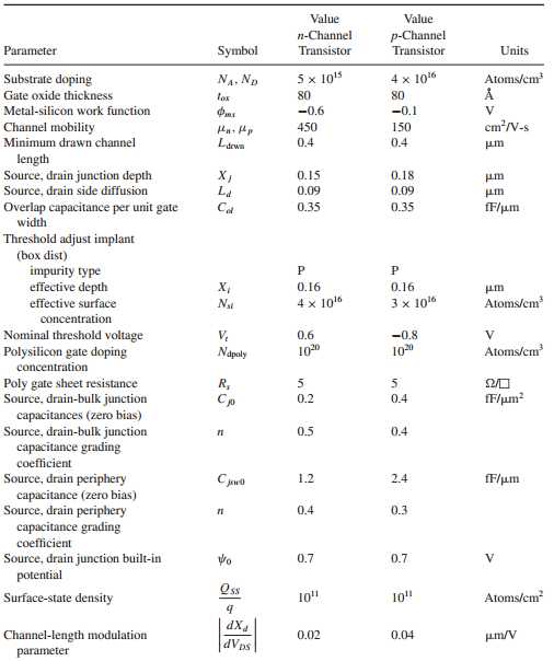
produces the bias voltagesVBIAS1, VBIAS2, and VBIAS3 based on IBIAS. The output current-drive capability is to be ± 100 μA, the output voltage-swing capability 1.5 Volts peak-peak, and the input common-mode range should extend from 0.5 V to the negative supply. Matching requirements dictate a minimum effective channel length of 1μm. To make the gain insensitive to small shifts in the operating point, design the circuit so that the magnitude of the drain-source voltage for each transistor operating in the active region exceeds the magnitude of its overdrive by at least 100 mV. Specify all device geometries and bias currents. The process is then-well process with parameters given in Table 2.4. Assume Xd =0 and γ = 0.25V ½ for both n- and p-channel transistors, but ignore the body effect in the hand calculations. Use SPICE to verify and refine your design as well as to determine the gain.
Figure 4.42
Table 2.4
VDp = 1.5 V 150 150 150 M7 M5 M8 Vi M2 M1 150 150 200 5 pF M6 100 50 50 -VDp = -1.5 V VDD M109 M103 M102, VBIAS1 M108 M104 M101 o VBIAS2 M105 o VBIAS3 IBIAS O M107, M106 -Vss
Step by Step Solution
3.52 Rating (169 Votes )
There are 3 Steps involved in it
For I 0max 100 A I D11 I D12 100 A Then half of I D11 should come from M 1 and the other half from M ... View full answer

Get step-by-step solutions from verified subject matter experts
Document Format (2 attachments)
1528_605d88e1b512f_686895.pdf
180 KBs PDF File
1528_605d88e1b512f_686895.docx
120 KBs Word File