

Question: Given the timing diagram in Figure P10.12 that is derived from the data sheet of a commercial SRAM, explain its action in words. FIGURE P10.12
Given the timing diagram in Figure P10.12 that is derived from the data sheet of a commercial SRAM, explain its action in words.
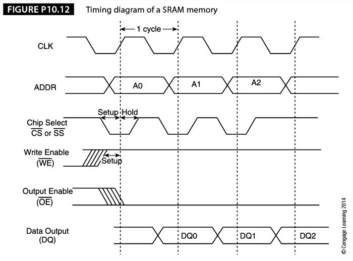
FIGURE P10.12 CLK ADDR Chip Select CS or SS Write Enable (WE) Output Enable (OE) Data Output (DQ) Timing diagram of a SRAM memory -1 cycle Setup Hold TILL'S AO Setup A1 DQ0 A2 DQ1 DQ2 Cengage Learning 2014
Step by Step Solution
★★★★★
3.37 Rating (144 Votes )
There are 3 Steps involved in it
1 Expert Approved Answer
Step: 1 Unlock

This is a read cycle because the write enable signal WE is inactivehigh i... View full answer
Question Has Been Solved by an Expert!
Get step-by-step solutions from verified subject matter experts
Step: 2 Unlock
Step: 3 Unlock