Question
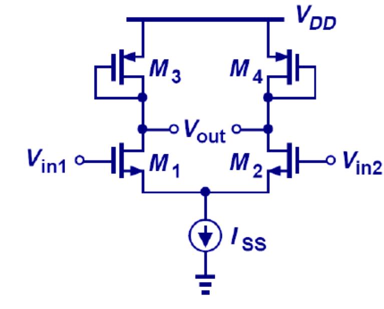
The circuit shown above is a MOS differential amplifier with the drain resistors RD implemented using diode-connected PMOS transistors, M3 and M4. Let M1


The circuit shown above is a MOS differential amplifier with the drain resistors RD implemented using diode-connected PMOS transistors, M3 and M4. Let M1 and M2 be matched, and M3 and M4 be matched. If X>0 and gm ro >> 1: (a) Use circuit splitting technique to derive an expression for the differential voltage gain (Ad) (b) Determine the common-mode gain (A_CM) assuming that the tail current source (Iss) is non-ideal so that it has a finite output resistance Rss (parallel with the tail current source) M3 M Vout Vin1 M M2 + Iss VDD Vin2
Step by Step Solution
3.36 Rating (152 Votes )
There are 3 Steps involved in it
Step: 1

Get Instant Access to Expert-Tailored Solutions
See step-by-step solutions with expert insights and AI powered tools for academic success
Step: 2

Step: 3

Ace Your Homework with AI
Get the answers you need in no time with our AI-driven, step-by-step assistance
Get StartedRecommended Textbook for
Analysis and Design of Analog Integrated Circuits
Authors: Paul R. Gray, Paul J. Hurst Stephen H. Lewis, Robert G. Meyer
5th edition
1111827052, 1285401107, 9781285401102 , 978-0470245996
Students also viewed these Electrical Engineering questions
Question
Answered: 1 week ago
Question
Answered: 1 week ago
Question
Answered: 1 week ago
Question
Answered: 1 week ago
Question
Answered: 1 week ago
Question
Answered: 1 week ago
Question
Answered: 1 week ago
Question
Answered: 1 week ago
Question
Answered: 1 week ago
Question
Answered: 1 week ago
Question
Answered: 1 week ago
Question
Answered: 1 week ago
Question
Answered: 1 week ago
Question
Answered: 1 week ago
Question
Answered: 1 week ago
Question
Answered: 1 week ago
Question
Answered: 1 week ago
Question
Answered: 1 week ago
Question
Answered: 1 week ago
Question
Answered: 1 week ago
Question
Answered: 1 week ago
Question
Answered: 1 week ago
Question
Answered: 1 week ago
View Answer in SolutionInn App


