

Question: Figure 7.24 shows the data path circuit for the shift-and-add multiplier. It uses a shift register for B so that b0 can be used to
Figure 7.24 shows the data path circuit for the shift-and-add multiplier. It uses a shift register for B so that b0 can be used to decide whether or not A should be added to P. A different approach is to use a normal register to hold operand B and to use a counter and multiplexer to select bit bi in each stage of the multiplication operation.
(a) Show the ASM chart that uses a normal register for B, instead of a shift register.
(b) Show the data path circuit corresponding to part (a).
(c) Give the ASM chart for the control circuit corresponding to part (b).
(d) Give Verilog code that represents the multiplier circuit.
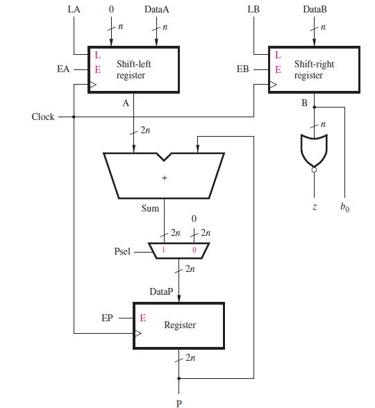
Clock LA EA E 0 fn EP Shift-left register A DataA fn Psel 2n Sum E 1 0 -2n +2n 0 DataP 2n Register P 2n LB EB [1] E DataB fn Shift-right register B Z bo
Step by Step Solution
3.33 Rating (168 Votes )
There are 3 Steps involved in it
The image provided shows the data path circuit for a shiftandadd multiplier used in digital systems to perform multiplication of binary numbers Typically this method of multiplication involves shiftin... View full answer

Get step-by-step solutions from verified subject matter experts