Answered step by step
Verified Expert Solution
Question
1 Approved Answer
1) Design using VHDL with EDA Playground, a 4 x 4-bit parallel multiplier using the correct number of adder blocks - full-adders (FAs) and

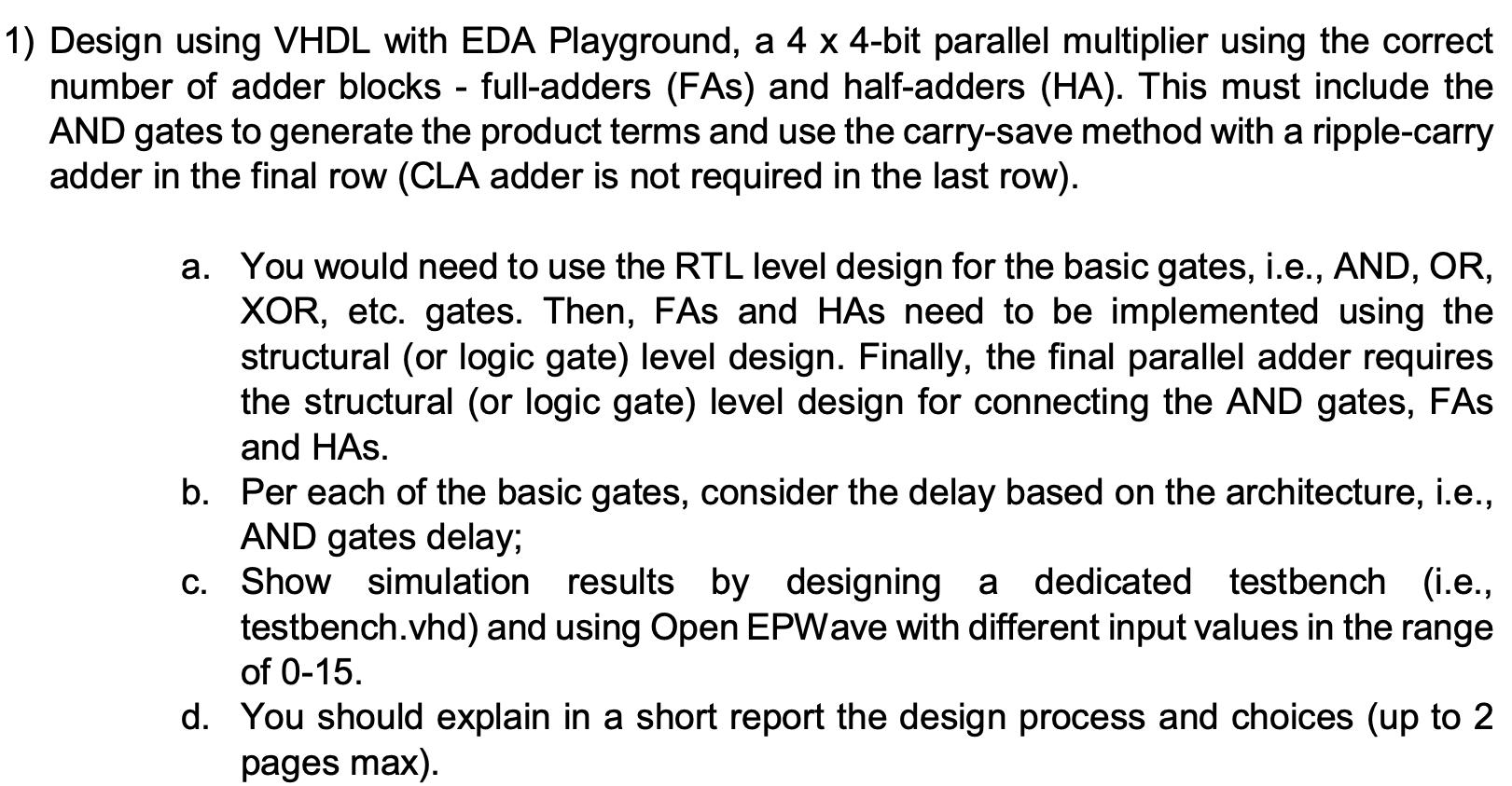
1) Design using VHDL with EDA Playground, a 4 x 4-bit parallel multiplier using the correct number of adder blocks - full-adders (FAs) and half-adders (HA). This must include the AND gates to generate the product terms and use the carry-save method with a ripple-carry adder in the final row (CLA adder is not required in the last row). a. You would need to use the RTL level design for the basic gates, i.e., AND, OR, XOR, etc. gates. Then, FAs and HAs need to be implemented using the structural (or logic gate) level design. Finally, the final parallel adder requires the structural (or logic gate) level design for connecting the AND gates, FAS and HAS. b. Per each of the basic gates, consider the delay based on the architecture, i.e., AND gates delay; c. Show simulation results by designing a dedicated testbench (i.e., testbench.vhd) and using Open EPWave with different input values in the range of 0-15. d. You should explain in a short report the design process and choices (up to 2 pages max).
Step by Step Solution
There are 3 Steps involved in it
Step: 1

Get Instant Access to Expert-Tailored Solutions
See step-by-step solutions with expert insights and AI powered tools for academic success
Step: 2

Step: 3

Ace Your Homework with AI
Get the answers you need in no time with our AI-driven, step-by-step assistance
Get Started


