Answered step by step
Verified Expert Solution
Question
1 Approved Answer
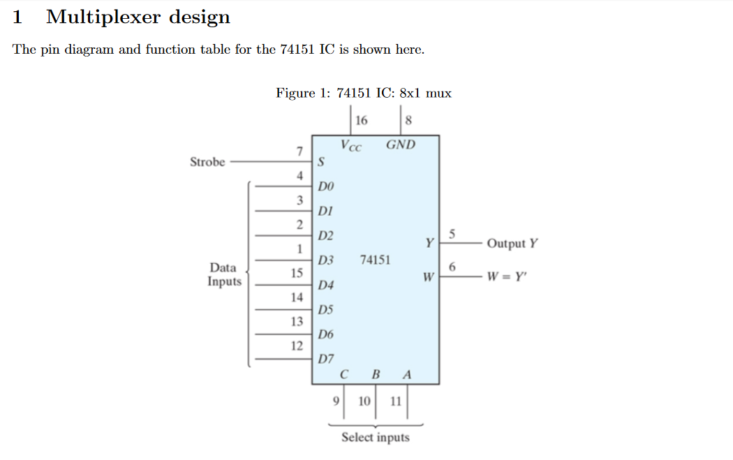
1 Multiplexer design The pin diagram and function table for the 74151 IC is shown here. Strobe Data Inputs Figure 1: 74151 IC: 8x1


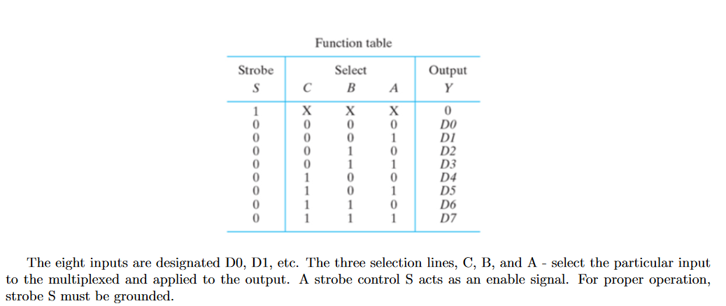
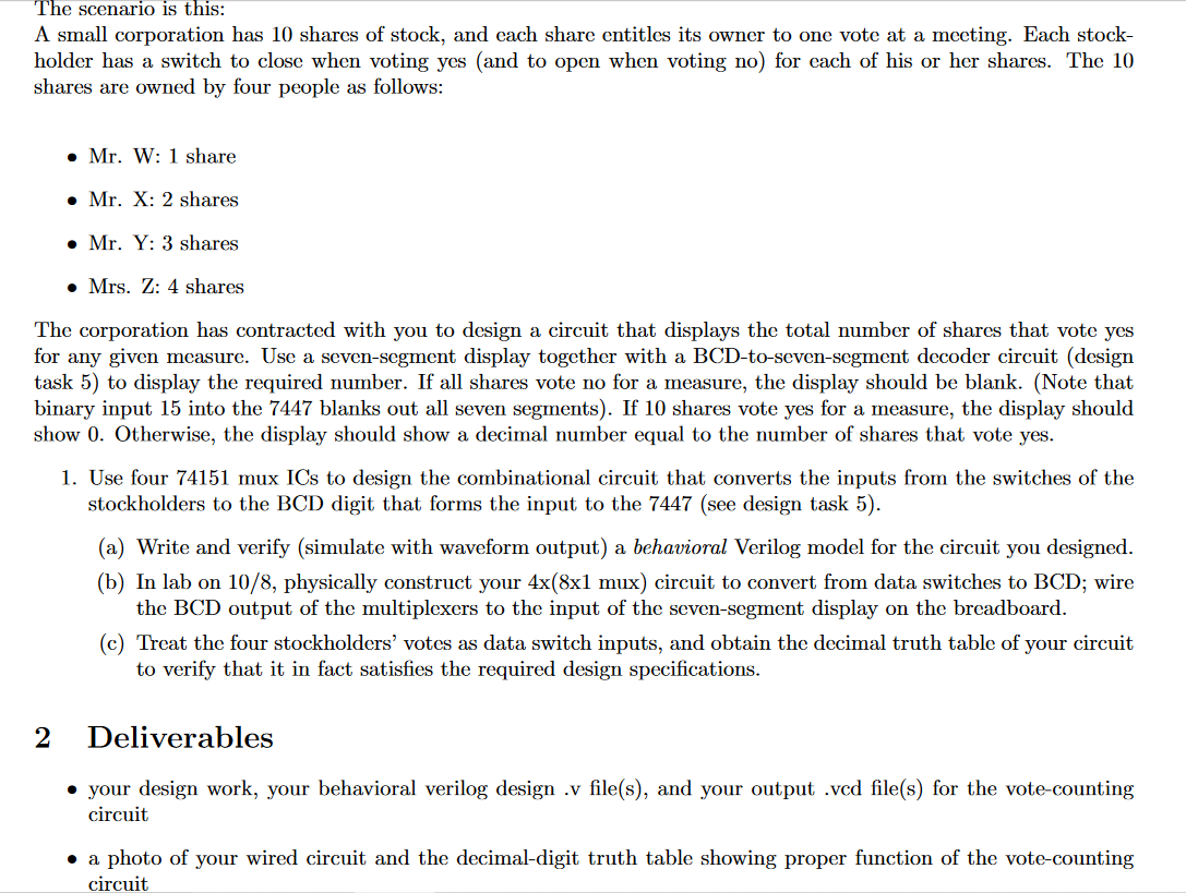
1 Multiplexer design The pin diagram and function table for the 74151 IC is shown here. Strobe Data Inputs Figure 1: 74151 IC: 8x1 mux 16 7 4 3 2 1 15 14 13 12 S DO DI D2 D3 D4 D5 D6 D7 Vcc C 9 GND 74151 8 BA 10 11 Select inputs Y W 5 6 Output Y W = Y' Strobe S 1 0 0 0 0 0 0 0 0 C X 0 0 0 0 1 1 1 1 Function table Select B X 0 0 1 1 0 0 1 1 A X 0 1 0 1 0 1 0 1 Output Y 0 DO DI D2 D3 D4 D5 D6 D7 The eight inputs are designated D0, D1, etc. The three selection lines, C, B, and A - select the particular input to the multiplexed and applied to the output. A strobe control S acts as an enable signal. For proper operation, strobe S must be grounded. The scenario is this: A small corporation has 10 shares of stock, and each share entitles its owner to one vote at a meeting. Each stock- holder has a switch to close when voting yes (and to open when voting no) for each of his or her shares. The 10 shares are owned by four people as follows: Mr. W: 1 share . Mr. X: 2 shares . Mr. Y: 3 shares . Mrs. Z: 4 shares The corporation has contracted with you to design a circuit that displays the total number of shares that vote yes for any given measure. Use a seven-segment display together with a BCD-to-seven-segment decoder circuit (design task 5) to display the required number. If all shares vote no for a measure, the display should be blank. (Note that binary input 15 into the 7447 blanks out all seven segments). If 10 shares vote yes for a measure, the display should show 0. Otherwise, the display should show a decimal number equal to the number of shares that vote yes. 2 1. Use four 74151 mux ICs to design the combinational circuit that converts the inputs from the switches of the stockholders to the BCD digit that forms the input to the 7447 (see design task 5). (a) Write and verify (simulate with waveform output) a behavioral Verilog model for the circuit you designed. (b) In lab on 10/8, physically construct your 4x(8x1 mux) circuit to convert from data switches to BCD; wire the BCD output of the multiplexers to the input of the seven-segment display on the breadboard. (c) Treat the four stockholders' votes as data switch inputs, and obtain the decimal truth table of your circuit to verify that it in fact satisfies the required design specifications. Deliverables your design work, your behavioral verilog design .v file(s), and your output .vcd file(s) for the vote-counting circuit a photo of your wired circuit and the decimal-digit truth table showing proper function of the vote-counting circuit
Step by Step Solution
There are 3 Steps involved in it
Step: 1
Answer Multiplixer table to the given function ABC ABC ABC ABC ABC ABC ABC ABC D 0 2 4 6 8 10 12 14 ...
Get Instant Access to Expert-Tailored Solutions
See step-by-step solutions with expert insights and AI powered tools for academic success
Step: 2

Step: 3

Ace Your Homework with AI
Get the answers you need in no time with our AI-driven, step-by-step assistance
Get Started


