Answered step by step
Verified Expert Solution
Question
1 Approved Answer
1 - Review the main steps for designing an embedded system. 2 - Explain the following: a ) Types Real Time Systems. b ) Design
Review the main steps for designing an embedded system.
Explain the following:
a Types Real Time Systems.
b Design metrics for Real Time Embedded Systems.
Explain the main differences between ASIP, FPGA, PLD and ASIC.
Define the processor technology and compare between single purpose processor, general purpose processor and application specific processor.
Identify the key differences between hard realtime, soft realtime and firm realtime systems. Give at least one example of real time tasks corresponding to these three categories. Identify the timing constraints in your tasks and justify why the tasks should be categorized into the categories you have indicated.
With the help of block diagram, explain the working of a typical embeddedconcurrent system for controlling a plant using microcontroller. The components of the system are:
a Microcontroller,
b Sensors
c Actuators
d DataControl bus
What is an Embedded system and what are its characteristics?
What are common design metrics for embedded systems?
Give three differences between RISC and CISC Architectures.
Find the following
aThe flags that are stored in the PSW
bWhich register holds the serial data interrupt bits TI and RI
cAddress of the stack when the is reset
dNumber of registers banks and their address
ePorts used for external memory access
fWhich port has no alternative functions
Write programs that will accomplish the desired tasks listed below, using as few lines of code as possible. Use only opcodes that have been covered in class. Comment on each line of code.
aPlace the number in internal RAM locations to
bCopy the data at internal RAM location Fh to R and R
cSet the SP at the byte address just above the last working register address
dExchange the contents of the SP and the PSW
fCopy the byte at internal RAM address to external RAM address
eCopy the content of DPTR to registers RDPL and RDPH
jCopy the data in external RAM location to TL and the data in external RAM location h to TH
hCopy the data in internal RAM locations to to internal RAM locations to ; copy to to etc..
iSet the SP register to and PUSH the SP register on the stack; predict what number is PUSHED to address
gExchange the content of the B register and external RAM address CFh
kRotate the bytes in registers to ; copy the data in to to to and to R
lCopy the external code byte at address to the SP
mCopy the data in register R to external RAM address
nCopy the internal code byte at address to external RAM address
oSwap the bytes in TIMER ; put TL in TH and TH in TL
pStore DPTR in external RAM locations h DPL and BCh DPH
qExchange both low nibbles of registers R and R; put the low nibble of R in R and the low nibble of in
rStore the content of register R at the internal RAM address contained in RBe sure the address in R is legal
sStore the content of RAM location at the address contained in RAM location
tStore register A at the internal RAM location address in register A
uCopy program bytes to to internal RAM locations to
vCopy the data on the pins of port p to the port latch
wPUSH the contents of the B register to TMOD
xCopy the contents of external code memory address h to IE
yShow a set of XCH instructions executes faster then PUSH and POP when saving the contents of the A register
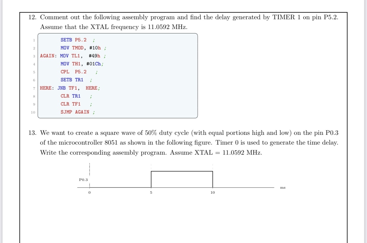
Comment out the following assembly program and find the delay generated by TIMER on pin P Assume that the XTAL frequency is
We want to create a square wave of duty cycle with equal portions high and low on the pin P of the microcontroller as shown in the following figure. Timer is used to generate the time delay. Write the corresponding assembly program. Assume XTAL MHz

Step by Step Solution
There are 3 Steps involved in it
Step: 1

Get Instant Access to Expert-Tailored Solutions
See step-by-step solutions with expert insights and AI powered tools for academic success
Step: 2

Step: 3

Ace Your Homework with AI
Get the answers you need in no time with our AI-driven, step-by-step assistance
Get Started


