Answered step by step
Verified Expert Solution
Question
1 Approved Answer
1. The equation for finding the ac emitter resistance of a BJT is a. Ve = 25 mV IB 25 mV IE 0.7 V
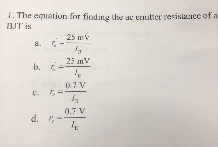
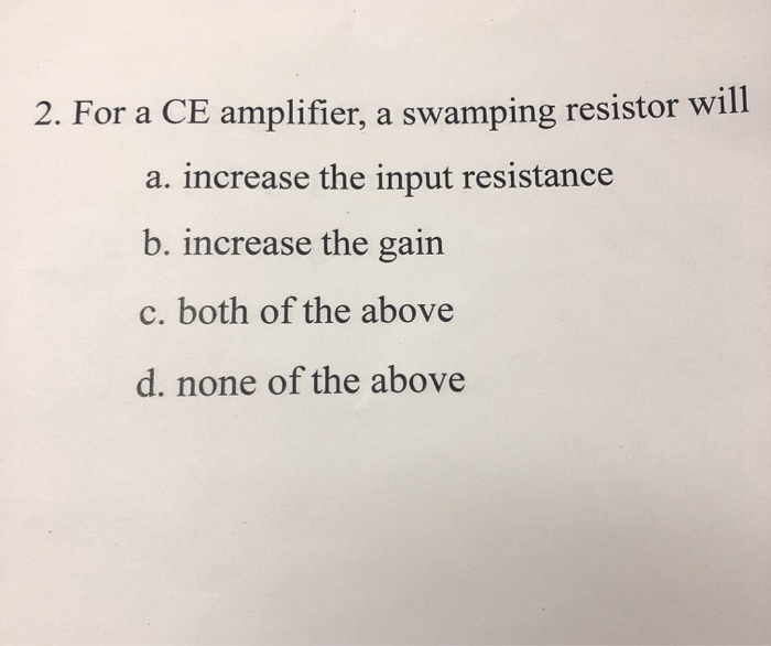
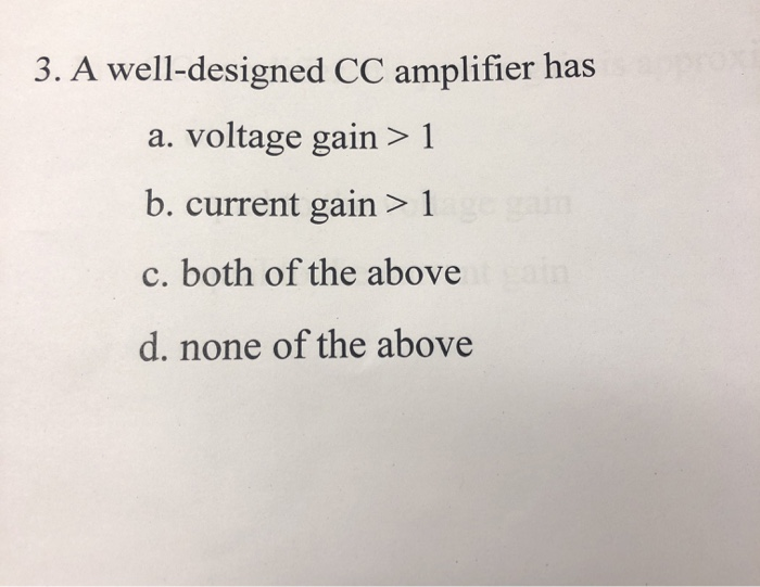
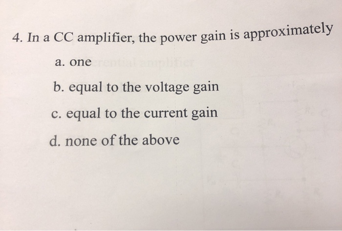
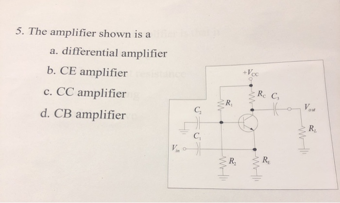
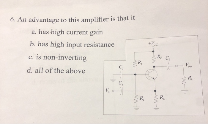
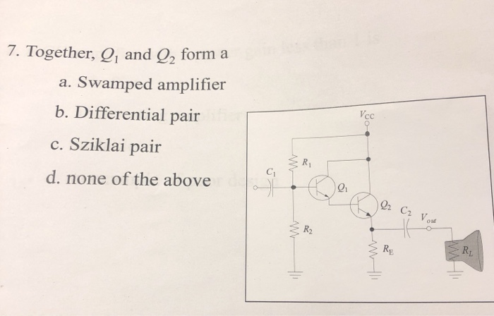
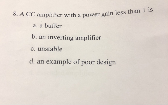
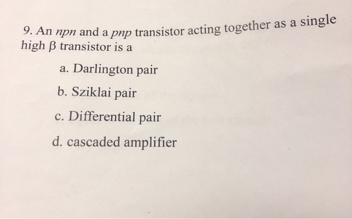
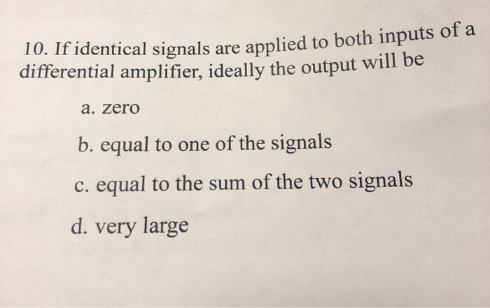
1. The equation for finding the ac emitter resistance of a BJT is a. Ve = 25 mV IB 25 mV IE 0.7 V IB 0.7 V IE b. bor =- C. r = re d. r=- 2. For a CE amplifier, a swamping resistor will a. increase the input resistance b. increase the gain c. both of the above d. none of the above 3. A well-designed CC amplifier has a. voltage gain> 1 b. current gain > 1 c. both of the above d. none of the above 4. In a CC amplifier, the power gain is approximately a. one b. equal to the voltage gain c. equal to the current gain d. none of the above 5. The amplifier shown is a a. differential amplifier b. CE amplifier c. CC amplifier d. CB amplifier Vin O C C ww R www- R +Vcc w Rc C, www- RE Vout R 6. An advantage to this amplifier is that it a. has high current gain b. has high input resistance c. is non-inverting d. all of the above O C C M R www- R +Vcc Re C w Ho You RE www- R 7. Together, Q and Q form a a. Swamped amplifier b. Differential pair c. Sziklai pair d. none of the above C www w R R Q Vcc ww1 102 C2 Vo RE R 8. A CC amplifier with a power gain less than 1 is a. a buffer b. an inverting amplifier c. unstable d. an example of poor design 9. An npn and a pnp transistor acting together as a single high transistor is a a. Darlington pair b. Sziklai pair c. Differential pair d. cascaded amplifier 10. If identical signals are applied to both inputs of a differential amplifier, ideally the output will be a. zero b. equal to one of the signals c. equal to the sum of the two signals d. very large 1. The equation for finding the ac emitter resistance of a BJT is a. Ve = 25 mV IB 25 mV IE 0.7 V IB 0.7 V IE b. bor =- C. r = re d. r=- 2. For a CE amplifier, a swamping resistor will a. increase the input resistance b. increase the gain c. both of the above d. none of the above 3. A well-designed CC amplifier has a. voltage gain> 1 b. current gain > 1 c. both of the above d. none of the above 4. In a CC amplifier, the power gain is approximately a. one b. equal to the voltage gain c. equal to the current gain d. none of the above 5. The amplifier shown is a a. differential amplifier b. CE amplifier c. CC amplifier d. CB amplifier Vin O C C ww R www- R +Vcc w Rc C, www- RE Vout R 6. An advantage to this amplifier is that it a. has high current gain b. has high input resistance c. is non-inverting d. all of the above O C C M R www- R +Vcc Re C w Ho You RE www- R 7. Together, Q and Q form a a. Swamped amplifier b. Differential pair c. Sziklai pair d. none of the above C www w R R Q Vcc ww1 102 C2 Vo RE R 8. A CC amplifier with a power gain less than 1 is a. a buffer b. an inverting amplifier c. unstable d. an example of poor design 9. An npn and a pnp transistor acting together as a single high transistor is a a. Darlington pair b. Sziklai pair c. Differential pair d. cascaded amplifier 10. If identical signals are applied to both inputs of a differential amplifier, ideally the output will be a. zero b. equal to one of the signals c. equal to the sum of the two signals d. very large 1. The equation for finding the ac emitter resistance of a BJT is a. Ve = 25 mV IB 25 mV IE 0.7 V IB 0.7 V IE b. bor =- C. r = re d. r=- 2. For a CE amplifier, a swamping resistor will a. increase the input resistance b. increase the gain c. both of the above d. none of the above 3. A well-designed CC amplifier has a. voltage gain> 1 b. current gain > 1 c. both of the above d. none of the above 4. In a CC amplifier, the power gain is approximately a. one b. equal to the voltage gain c. equal to the current gain d. none of the above 5. The amplifier shown is a a. differential amplifier b. CE amplifier c. CC amplifier d. CB amplifier Vin O C C ww R www- R +Vcc w Rc C, www- RE Vout R 6. An advantage to this amplifier is that it a. has high current gain b. has high input resistance c. is non-inverting d. all of the above O C C M R www- R +Vcc Re C w Ho You RE www- R 7. Together, Q and Q form a a. Swamped amplifier b. Differential pair c. Sziklai pair d. none of the above C www w R R Q Vcc ww1 102 C2 Vo RE R 8. A CC amplifier with a power gain less than 1 is a. a buffer b. an inverting amplifier c. unstable d. an example of poor design 9. An npn and a pnp transistor acting together as a single high transistor is a a. Darlington pair b. Sziklai pair c. Differential pair d. cascaded amplifier 10. If identical signals are applied to both inputs of a differential amplifier, ideally the output will be a. zero b. equal to one of the signals c. equal to the sum of the two signals d. very large 1. The equation for finding the ac emitter resistance of a BJT is a. Ve = 25 mV IB 25 mV IE 0.7 V IB 0.7 V IE b. bor =- C. r = re d. r=- 2. For a CE amplifier, a swamping resistor will a. increase the input resistance b. increase the gain c. both of the above d. none of the above 3. A well-designed CC amplifier has a. voltage gain> 1 b. current gain > 1 c. both of the above d. none of the above 4. In a CC amplifier, the power gain is approximately a. one b. equal to the voltage gain c. equal to the current gain d. none of the above 5. The amplifier shown is a a. differential amplifier b. CE amplifier c. CC amplifier d. CB amplifier Vin O C C ww R www- R +Vcc w Rc C, www- RE Vout R 6. An advantage to this amplifier is that it a. has high current gain b. has high input resistance c. is non-inverting d. all of the above O C C M R www- R +Vcc Re C w Ho You RE www- R 7. Together, Q and Q form a a. Swamped amplifier b. Differential pair c. Sziklai pair d. none of the above C www w R R Q Vcc ww1 102 C2 Vo RE R 8. A CC amplifier with a power gain less than 1 is a. a buffer b. an inverting amplifier c. unstable d. an example of poor design 9. An npn and a pnp transistor acting together as a single high transistor is a a. Darlington pair b. Sziklai pair c. Differential pair d. cascaded amplifier 10. If identical signals are applied to both inputs of a differential amplifier, ideally the output will be a. zero b. equal to one of the signals c. equal to the sum of the two signals d. very large 1. The equation for finding the ac emitter resistance of a BJT is a. Ve = 25 mV IB 25 mV IE 0.7 V IB 0.7 V IE b. bor =- C. r = re d. r=- 2. For a CE amplifier, a swamping resistor will a. increase the input resistance b. increase the gain c. both of the above d. none of the above 3. A well-designed CC amplifier has a. voltage gain> 1 b. current gain > 1 c. both of the above d. none of the above 4. In a CC amplifier, the power gain is approximately a. one b. equal to the voltage gain c. equal to the current gain d. none of the above 5. The amplifier shown is a a. differential amplifier b. CE amplifier c. CC amplifier d. CB amplifier Vin O C C ww R www- R +Vcc w Rc C, www- RE Vout R 6. An advantage to this amplifier is that it a. has high current gain b. has high input resistance c. is non-inverting d. all of the above O C C M R www- R +Vcc Re C w Ho You RE www- R 7. Together, Q and Q form a a. Swamped amplifier b. Differential pair c. Sziklai pair d. none of the above C www w R R Q Vcc ww1 102 C2 Vo RE R 8. A CC amplifier with a power gain less than 1 is a. a buffer b. an inverting amplifier c. unstable d. an example of poor design 9. An npn and a pnp transistor acting together as a single high transistor is a a. Darlington pair b. Sziklai pair c. Differential pair d. cascaded amplifier 10. If identical signals are applied to both inputs of a differential amplifier, ideally the output will be a. zero b. equal to one of the signals c. equal to the sum of the two signals d. very large
Step by Step Solution
★★★★★
3.43 Rating (159 Votes )
There are 3 Steps involved in it
Step: 1

Get Instant Access to Expert-Tailored Solutions
See step-by-step solutions with expert insights and AI powered tools for academic success
Step: 2

Step: 3

Ace Your Homework with AI
Get the answers you need in no time with our AI-driven, step-by-step assistance
Get Started


