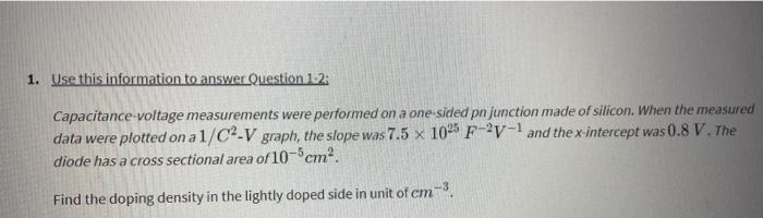
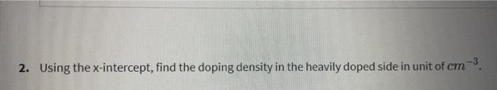
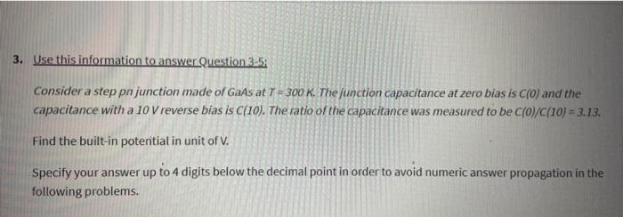
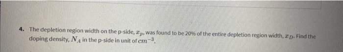
1. Use this information to answer Question 1.2i Capacitance-voltage measurements were performed on a one-sided pn junction made of silicon. When the measured data were plotted on a 1/C2V graph, the slope was 7.51025F2V1 and the -intercept was 0.8V. The diode has a cross sectional area of 105cm2. Find the doping density in the lightly doped side in unit of cm3. 2. Using the x-intercept, find the doping density in the heavily doped side in unit of cm3. 3. Use this information to answerQuestion 3-5: Consider a step pn junction made of GaAs at T=300K. The junction capacitance at zero bias is C(0) and the capacitance with a 10V reverse bias is C(10). The ratio of the capacitance was measured to be C(0)/C(10)=3,13. Find the built-in potenitial in unit of V. Specify your answer up to 4 digits below the decimal point in order to avoid numeric answer propagation in the. following problems. 4. The depletion region width on the p-side, xp, was found to be 20% of the entire depletion region width, xD. Find the doping density, NA in the p-side in unit of cm3. 5. Find the doping density, ND in the n-side in unit of cm3. 6. Use this information to answerQuestion 6-8: Consider a one-sided step pn junction made of silicon in which the doping density in the n-side is much greater than that in the p-side, ND>>NA. This junction is under a reverse bias of 10V. If the doping density, NA, in the p-side is doubled, what would be the percent change in junction capacitance, c? 7. Also, calculate the change in the built-in potential, i, in unit of V. 8. Use this information to answer Question 8-9: A silicon pn junction (step junction) has doping densities of NA=51015cm3 on the p-side and ND=11017cm3 on the n-side. Carrier lifetimes are given as n=106s and p=107s. Assume long diode, i.e. long quasi-neutral regions. Calculate the current density in A/cm2 at a forward bias of Va=0.5V. 9. Calculate the ratio of hole current density to total current density at the depletion region edge, xn, on the n-side. 10. Considera step pn junction made of silicon. Carrier lifetimes are given as n=107s and p=107s. Assume Iong diode, i.e. long quasi-neutral regions. What must be the doping density ratio, NA/ND, in order to have 95% of the total current in the depletion region carried by electrons? 11. Consider two ideal pn junctions at T=300K with exactly the same physical parameters except for the bandgap energy. The first pn junction has a bandgap energy of 0.525eV and a forward current of J1=10mA at Va=0.255V. For the second pn junction, a forward current of J2=10A was measured at Va=0.32V. What is the bandgap energy of the second pn junction material? Give your answer in unit of eV 12. Use this information to answer Question 12-16: A silicon pn junction (step junction) has doping densities of NA=11016cm3 on the p-sideand ND=21016cm3 on the n-side. Carrier lifetimes are given as n=106s and p=108s. Assume long diode, i.e. long quasi-neutral regions. Calculate the built-in voltage in unit of V. 13. Suppose now that a forward bias of 0.6V is applied. Calculate the minority carrier concentration, np, at the edge of the depletion region on the p-side, x=xp. Give your answer in unit of cm3. 14. Under a forward bias of 0.6V, calculate the minority carrier concentration, pn, at the edge of the depletion region on then-side, x=xn. Give your answer in unit of cm3 15. Under a forward bias of 0.6V, calculate the current density, Jtotal, in unit of A/cm2. 1. Use this information to answer Question 1.2i Capacitance-voltage measurements were performed on a one-sided pn junction made of silicon. When the measured data were plotted on a 1/C2V graph, the slope was 7.51025F2V1 and the -intercept was 0.8V. The diode has a cross sectional area of 105cm2. Find the doping density in the lightly doped side in unit of cm3. 2. Using the x-intercept, find the doping density in the heavily doped side in unit of cm3. 3. Use this information to answerQuestion 3-5: Consider a step pn junction made of GaAs at T=300K. The junction capacitance at zero bias is C(0) and the capacitance with a 10V reverse bias is C(10). The ratio of the capacitance was measured to be C(0)/C(10)=3,13. Find the built-in potenitial in unit of V. Specify your answer up to 4 digits below the decimal point in order to avoid numeric answer propagation in the. following problems. 4. The depletion region width on the p-side, xp, was found to be 20% of the entire depletion region width, xD. Find the doping density, NA in the p-side in unit of cm3. 5. Find the doping density, ND in the n-side in unit of cm3. 6. Use this information to answerQuestion 6-8: Consider a one-sided step pn junction made of silicon in which the doping density in the n-side is much greater than that in the p-side, ND>>NA. This junction is under a reverse bias of 10V. If the doping density, NA, in the p-side is doubled, what would be the percent change in junction capacitance, c? 7. Also, calculate the change in the built-in potential, i, in unit of V. 8. Use this information to answer Question 8-9: A silicon pn junction (step junction) has doping densities of NA=51015cm3 on the p-side and ND=11017cm3 on the n-side. Carrier lifetimes are given as n=106s and p=107s. Assume long diode, i.e. long quasi-neutral regions. Calculate the current density in A/cm2 at a forward bias of Va=0.5V. 9. Calculate the ratio of hole current density to total current density at the depletion region edge, xn, on the n-side. 10. Considera step pn junction made of silicon. Carrier lifetimes are given as n=107s and p=107s. Assume Iong diode, i.e. long quasi-neutral regions. What must be the doping density ratio, NA/ND, in order to have 95% of the total current in the depletion region carried by electrons? 11. Consider two ideal pn junctions at T=300K with exactly the same physical parameters except for the bandgap energy. The first pn junction has a bandgap energy of 0.525eV and a forward current of J1=10mA at Va=0.255V. For the second pn junction, a forward current of J2=10A was measured at Va=0.32V. What is the bandgap energy of the second pn junction material? Give your answer in unit of eV 12. Use this information to answer Question 12-16: A silicon pn junction (step junction) has doping densities of NA=11016cm3 on the p-sideand ND=21016cm3 on the n-side. Carrier lifetimes are given as n=106s and p=108s. Assume long diode, i.e. long quasi-neutral regions. Calculate the built-in voltage in unit of V. 13. Suppose now that a forward bias of 0.6V is applied. Calculate the minority carrier concentration, np, at the edge of the depletion region on the p-side, x=xp. Give your answer in unit of cm3. 14. Under a forward bias of 0.6V, calculate the minority carrier concentration, pn, at the edge of the depletion region on then-side, x=xn. Give your answer in unit of cm3 15. Under a forward bias of 0.6V, calculate the current density, Jtotal, in unit of A/cm2