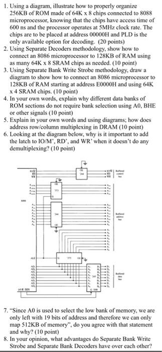
1. Using a diagram, illustrate how to properly organize 256KB of ROM made of 64K x 8 chips connected to 8088 microprocessor, knowing that the chips have access time of 600 ns and the processor operates at 5MHz clock rate. The chips are to be placed at address 00000H and PLD is the only available option for decoding. (20 points) 2. Using Separate Decoders methodology, show how to connect an 8086 microprocessor to 128KB of RAM using as many 64K x 8 SRAM chips as needed. (10 point) 3. Using Separate Bank Write Strobe methodology, draw a diagram to show how to connect an 8086 microprocessor to 128KB of RAM starting at address E0000H and using 64K x 4 SRAM chips. (10 point) 4. In your own words, explain why different data banks of ROM sections do not require bank selection using AO, BHE or other signals (10 point) 5. Explain in your own words and using diagrams: how does address row/column multiplexing in DRAM (10 point) 6. Looking at the diagram below, why is it important to add the latch to 10/M, RD', and WR when it doesn't do any demultiplexing? (10 point) . 1222222 ALI 4 7. "Since AO is used to select the low bank of memory, we are only left with 19 bits of address and therefore we can only map 512KB of memory", do you agree with that statement and why? (10 point) 8. In your opinion, what advantages do Separate Bank Write Strobe and Separate Bank Decoders have over each other? 1. Using a diagram, illustrate how to properly organize 256KB of ROM made of 64K x 8 chips connected to 8088 microprocessor, knowing that the chips have access time of 600 ns and the processor operates at 5MHz clock rate. The chips are to be placed at address 00000H and PLD is the only available option for decoding. (20 points) 2. Using Separate Decoders methodology, show how to connect an 8086 microprocessor to 128KB of RAM using as many 64K x 8 SRAM chips as needed. (10 point) 3. Using Separate Bank Write Strobe methodology, draw a diagram to show how to connect an 8086 microprocessor to 128KB of RAM starting at address E0000H and using 64K x 4 SRAM chips. (10 point) 4. In your own words, explain why different data banks of ROM sections do not require bank selection using AO, BHE or other signals (10 point) 5. Explain in your own words and using diagrams: how does address row/column multiplexing in DRAM (10 point) 6. Looking at the diagram below, why is it important to add the latch to 10/M, RD', and WR when it doesn't do any demultiplexing? (10 point) . 1222222 ALI 4 7. "Since AO is used to select the low bank of memory, we are only left with 19 bits of address and therefore we can only map 512KB of memory", do you agree with that statement and why? (10 point) 8. In your opinion, what advantages do Separate Bank Write Strobe and Separate Bank Decoders have over each other