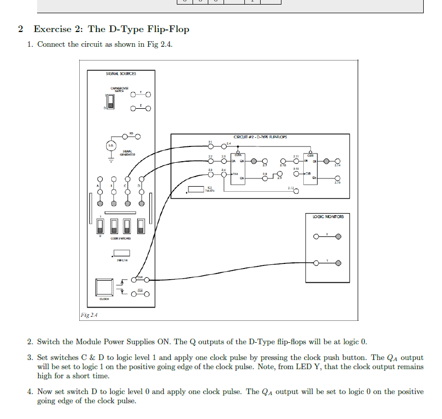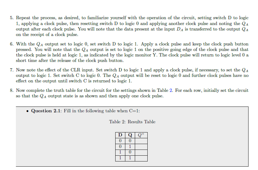

2 Exercise 2: The D-Type Flip-Flop 1. Connect the circuit as shown in Fig 2.4. SENAL SOURCES CHANEROV SAC obo CRUN #2-D-TYPE R RFLOPS SA GENEADO 26 CA 2.13 0.00 000 TE LOGIC MONTORS COCE SWRMES 70610 CLOCK Fig 2.4 2. Switch the Module Power Supplies ON. The Q outputs of the D-Type flip-flops will be at logic 0. 3. Set switches C & D to logic level 1 and apply one clock pulse by pressing the clock push button. The QA output will be set to logic 1 on the positive going edge of the clock pulse. Note, from LED Y, that the clock output remains high for a short time. 4. Now set switch D to logic level 0 and apply one clock pulse. The QA output will be set to logic 0 on the positive going edge of the clock pulse. a 5. Repeat the process, as desired, to familiarize yourself with the operation of the circuit, setting switch D to logic 1, applying a clock pulse, then resetting switch D to logic 0 and applying another clock pulse and noting the QA output after each clock pulse. You will note that the data present at the input DA is transferred to the output QA on the receipt of a clock pulse. 6. With the QA output set to logic 0, set switch D to logic 1. Apply a clock pulse and keep the clock push button pressed. You will note that the QA output is set to logic 1 on the positive going edge of the clock pulse and that the clock pulse is held at logic 1, as indicated by the logic monitor Y. The clock pulse will return to logic level 0 a short time after the release of the clock push button. 7. Now note the effect of the CLR input. Set switch D to logic 1 and apply a clock pulse, if necessary, to set the QA output to logic 1. Set switch C to logic 0. The QA output will be reset to logic 0 and further clock pulses have no effect on the output until switch C is returned to logic 1. 8. Now complete the truth table for the circuit for the settings shown in Table 2. For each row, initially set the circuit so that the QA output state is as shown and then apply one clock pulse. Question 2.1: Fill in the following table when C=1: Table 2: Results Table DQQ+ 0 0 0 1 1 0 1 Olo 2 Exercise 2: The D-Type Flip-Flop 1. Connect the circuit as shown in Fig 2.4. SENAL SOURCES CHANEROV SAC obo CRUN #2-D-TYPE R RFLOPS SA GENEADO 26 CA 2.13 0.00 000 TE LOGIC MONTORS COCE SWRMES 70610 CLOCK Fig 2.4 2. Switch the Module Power Supplies ON. The Q outputs of the D-Type flip-flops will be at logic 0. 3. Set switches C & D to logic level 1 and apply one clock pulse by pressing the clock push button. The QA output will be set to logic 1 on the positive going edge of the clock pulse. Note, from LED Y, that the clock output remains high for a short time. 4. Now set switch D to logic level 0 and apply one clock pulse. The QA output will be set to logic 0 on the positive going edge of the clock pulse. a 5. Repeat the process, as desired, to familiarize yourself with the operation of the circuit, setting switch D to logic 1, applying a clock pulse, then resetting switch D to logic 0 and applying another clock pulse and noting the QA output after each clock pulse. You will note that the data present at the input DA is transferred to the output QA on the receipt of a clock pulse. 6. With the QA output set to logic 0, set switch D to logic 1. Apply a clock pulse and keep the clock push button pressed. You will note that the QA output is set to logic 1 on the positive going edge of the clock pulse and that the clock pulse is held at logic 1, as indicated by the logic monitor Y. The clock pulse will return to logic level 0 a short time after the release of the clock push button. 7. Now note the effect of the CLR input. Set switch D to logic 1 and apply a clock pulse, if necessary, to set the QA output to logic 1. Set switch C to logic 0. The QA output will be reset to logic 0 and further clock pulses have no effect on the output until switch C is returned to logic 1. 8. Now complete the truth table for the circuit for the settings shown in Table 2. For each row, initially set the circuit so that the QA output state is as shown and then apply one clock pulse. Question 2.1: Fill in the following table when C=1: Table 2: Results Table DQQ+ 0 0 0 1 1 0 1 Olo


