Answered step by step
Verified Expert Solution
Question
1 Approved Answer
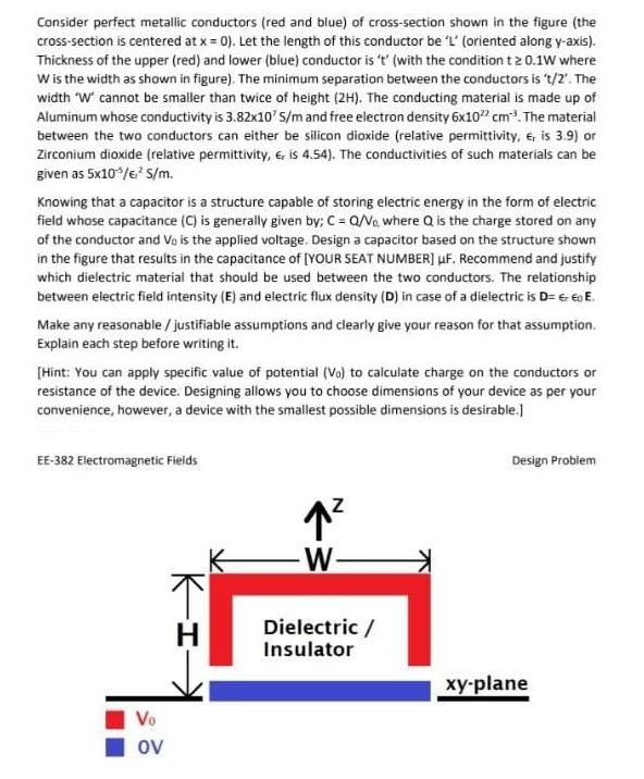
Consider perfect metallic conductors (red and blue) of cross-section shown in the figure (the cross-section is centered at x = 0). Let the length

Consider perfect metallic conductors (red and blue) of cross-section shown in the figure (the cross-section is centered at x = 0). Let the length of this conductor be 'L' (oriented along y-axis). Thckness of the upper (red) and lower (blue) conductor is 't' (with the condition t2 0.1W where W is the width as shown in figure). The minimum separation between the conductors is 't/2'. The width "W' cannot be smaller than twice of height (2H). The conducting material is made up of Aluminum whose conductivity is 3.82x10' /m and free electron density 6x10" cm. The material between the two conductors can either be silicon dioxide (relative permittivity, e, is 3.9) or Zirconium dioxide (relative permittivity, e, is 4.54). The conductivities of such materials can be given as 5x10*/e S/m. Knowing that a capacitor is a structure capable of storing electric energy in the form of electric field whose capacitance (C) is generally given by; C = QNa, where Q is the charge stored on any of the conductor and Va is the applied voltage. Design a capacitor based on the structure shown in the figure that results in the capacitance of [YOUR SEAT NUMBER) uF. Recommend and justify which dielectric material that should be used between the two conductors. The relationship between electric field intensity (E) and electric flux density (D) in case of a dielectric is D= E o E. Make any reasonable / justifiable assumptions and clearly give your reason for that assumption. Explain each step before writing it. [Hint: You can apply specific value of potential (Vo) to calculate charge on the conductors or resistance of the device. Designing allows you to choose dimensions of your device as per your convenience, however, a device with the smallest possible dimensions is desirable.) EE-382 Electromagnetic Fields Design Problem -W- Dielectric / Insulator xy-plane Vo ov KI-
Step by Step Solution
★★★★★
3.41 Rating (151 Votes )
There are 3 Steps involved in it
Step: 1

Get Instant Access to Expert-Tailored Solutions
See step-by-step solutions with expert insights and AI powered tools for academic success
Step: 2

Step: 3

Ace Your Homework with AI
Get the answers you need in no time with our AI-driven, step-by-step assistance
Get Started


