

Question: 2.2. Complete the truth table for the transistor level schematic shown in Fig.1. Also show the source of 'good' logic 0's and I's (using
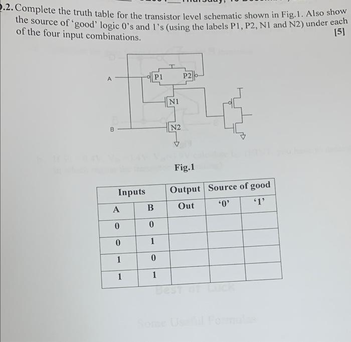
2.2. Complete the truth table for the transistor level schematic shown in Fig.1. Also show the source of 'good' logic 0's and I's (using the labels P1, P2, N1 and N2) under each of the four input combinations. [5] A B Inputs A 0 0 1 1 P1 B 0 |NI N2 P2 Fig.1 Output Source of good Out '0' '1' 1 0 1 best at LUCK
Step by Step Solution
★★★★★
3.39 Rating (152 Votes )
There are 3 Steps involved in it
1 Expert Approved Answer
Step: 1 Unlock

Truth table for the transistor level schematic shown in Fig 1 A B Outpu... View full answer
Question Has Been Solved by an Expert!
Get step-by-step solutions from verified subject matter experts
Step: 2 Unlock
Step: 3 Unlock