

Answered step by step
Verified Expert Solution
Question
1 Approved Answer
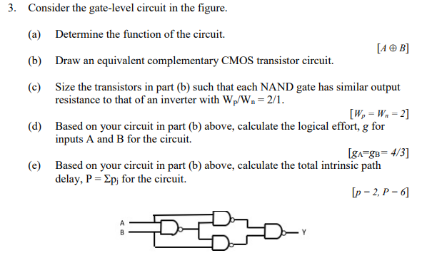
3. Consider the gate-level circuit in the figure. (a) Determine the function of the circuit. [AB] (b) Draw an equivalent complementary CMOS transistor circuit. (c)
Step by Step Solution
There are 3 Steps involved in it
Step: 1

Get Instant Access to Expert-Tailored Solutions
See step-by-step solutions with expert insights and AI powered tools for academic success
Step: 2

Step: 3
Ace Your Homework with AI
Get the answers you need in no time with our AI-driven, step-by-step assistance
Get Started
Database Processing
Authors: David M. Kroenke
12th Edition International Edition
1292023422, 978-1292023427