Answered step by step
Verified Expert Solution
Question
1 Approved Answer
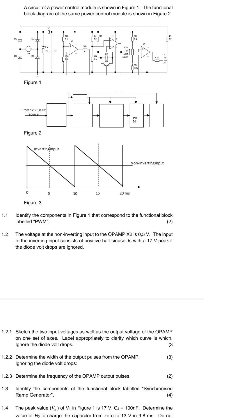
1.1 1.2 D2. A circuit of a power control module is shown in Figure 1. The functional block diagram of the same power control

1.1 1.2 D2. A circuit of a power control module is shown in Figure 1. The functional block diagram of the same power control module is shown in Figure 2. 1.4 V1 D3 D5 Figure 1 0 From 12 V 50 Hz Source Figure 2 D1 - Figure 3 LC1 Inverting input R2 10k 50% 10k 1 R7 --- C2 VR1 12k 500m R9 5 12k R8 10 15 20 ms 1K 1K R10 PW M R11 Non-inverting input R5 Identify the components in Figure 1 that correspond to the functional block labelled "PWM". (2) The voltage at the non-inverting input to the OPAMP X2 is 0,5 V. The input to the inverting input consists of positive half-sinusoids with a 17 V peak if the diode volt drops are ignored. 1.2.1 Sketch the two input voltages as well as the output voltage of the OPAMP on one set of axes. Label appropriately to clarify which curve is which. Ignore the diode volt drops. (3 (3) 1.2.2 Determine the width of the output pulses from the OPAMP. Ignoring the diode volt drops: 1.2.3 Determine the frequency of the OPAMP output pulses. 1.3 Identify the components of the functional block labelled "Synchronised Ramp Generator". (2) (4) The peak value (V) of V in Figure 1 is 17 V, C2 = 100nF. Determine the value of R3 to charge the capacitor from zero to 13 V in 9.8 ms. Do not
Step by Step Solution
There are 3 Steps involved in it
Step: 1
Sole G 83 RLS NIS 5 YIS RIS s 15 HIS Gs Ays 4115 s Ys RS Gls G 5 ...
Get Instant Access to Expert-Tailored Solutions
See step-by-step solutions with expert insights and AI powered tools for academic success
Step: 2

Step: 3

Ace Your Homework with AI
Get the answers you need in no time with our AI-driven, step-by-step assistance
Get Started


