Question
4.2 Consider a silicon PN step junction diode with Nd=1016cm and N = 5 x 105cm-. Assume T = 300 K. (a) Calculate the

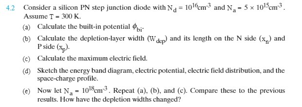
4.2 Consider a silicon PN step junction diode with Nd=1016cm and N = 5 x 105cm-. Assume T = 300 K. (a) Calculate the built-in potential bi (b) Calculate the depletion-layer width (W dep) and its length on the N side (x) and P side (xp). Calculate the maximum electric field. (c) (d) Sketch the energy band diagram, electric potential, electric field distribution, and the space-charge profile. (e) Now let N = 108 cm-3. Repeat (a), (b), and (c). Compare these to the previous results. How have the depletion widths changed?
Step by Step Solution
There are 3 Steps involved in it
Step: 1
ANSWER a To calculate the builtin potential Vbi we can use the formula Vbi kTq lnNaNdni2ight Given N...
Get Instant Access to Expert-Tailored Solutions
See step-by-step solutions with expert insights and AI powered tools for academic success
Step: 2

Step: 3

Ace Your Homework with AI
Get the answers you need in no time with our AI-driven, step-by-step assistance
Get StartedRecommended Textbook for
Analysis and Design of Analog Integrated Circuits
Authors: Paul R. Gray, Paul J. Hurst Stephen H. Lewis, Robert G. Meyer
5th edition
1111827052, 1285401107, 9781285401102 , 978-0470245996
Students also viewed these Business Communication questions
Question
Answered: 1 week ago
Question
Answered: 1 week ago
Question
Answered: 1 week ago
Question
Answered: 1 week ago
Question
Answered: 1 week ago
Question
Answered: 1 week ago
Question
Answered: 1 week ago
Question
Answered: 1 week ago
Question
Answered: 1 week ago
Question
Answered: 1 week ago
Question
Answered: 1 week ago
Question
Answered: 1 week ago
Question
Answered: 1 week ago
Question
Answered: 1 week ago
Question
Answered: 1 week ago
Question
Answered: 1 week ago
Question
Answered: 1 week ago
Question
Answered: 1 week ago
Question
Answered: 1 week ago
Question
Answered: 1 week ago
View Answer in SolutionInn App


