Question: ( 6) Assume that 16-bit datal in hexadecimal format is (#0x457F) and 16-bit data2 in hexadecimal format is (#OxAB36). Answer the following: i) Assume the
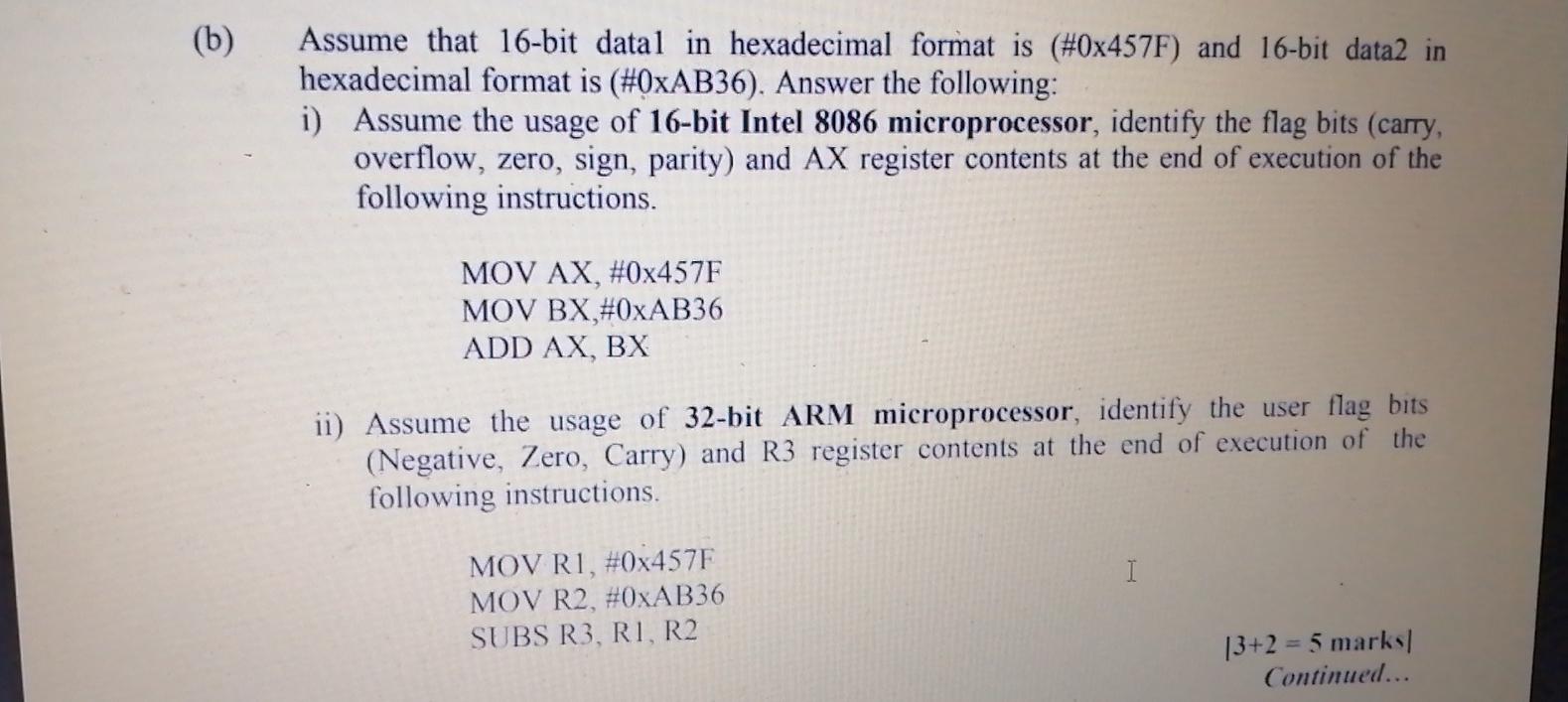
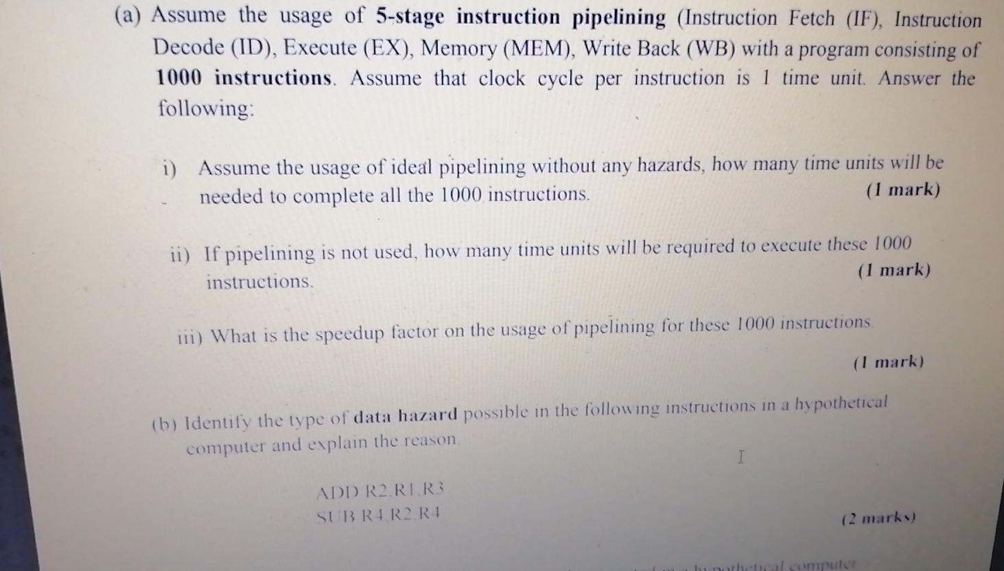
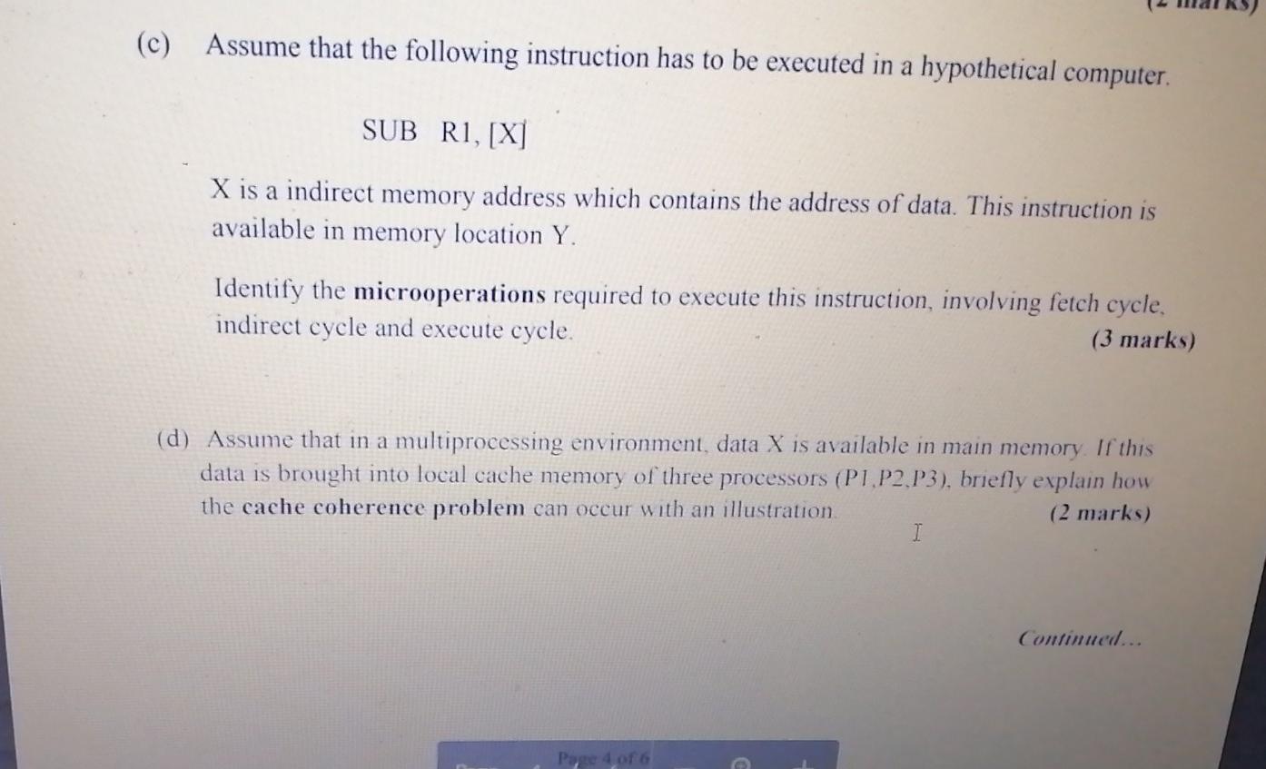
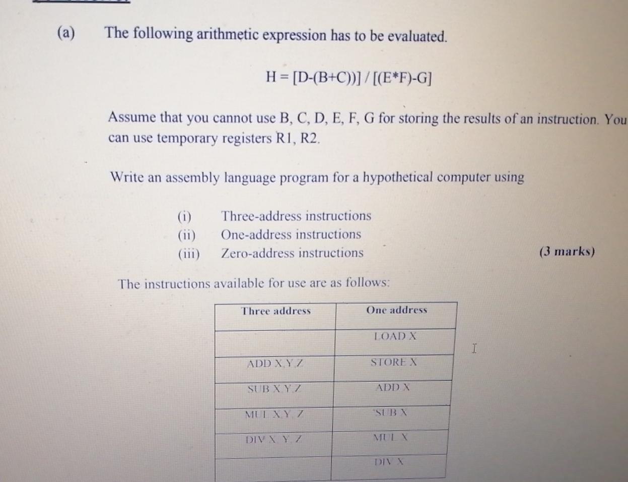
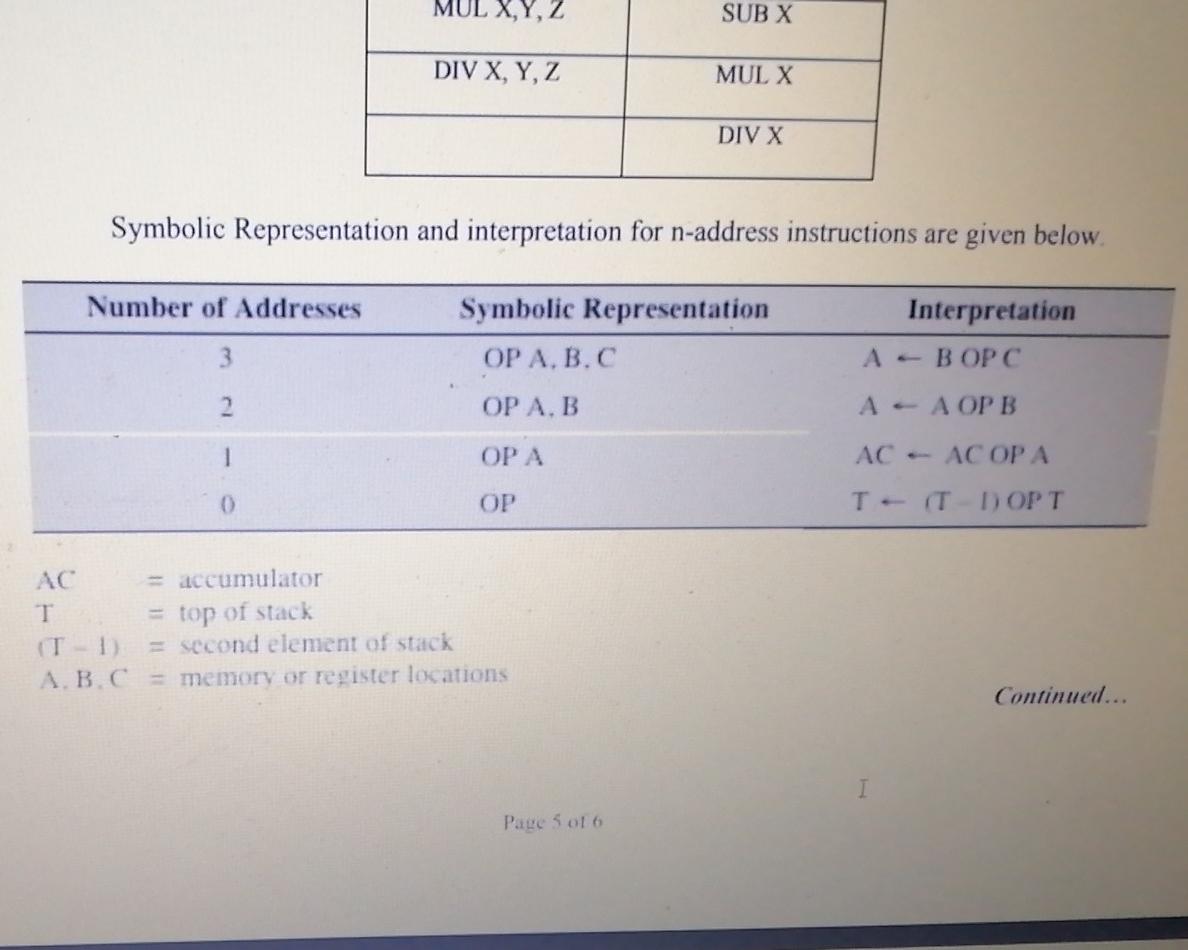
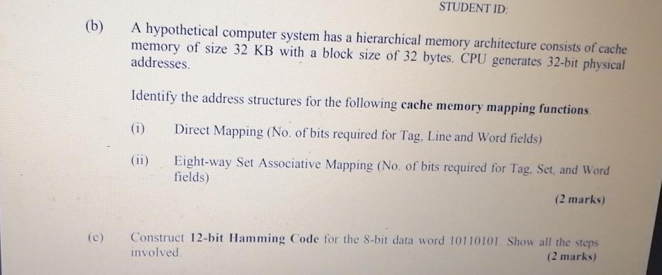
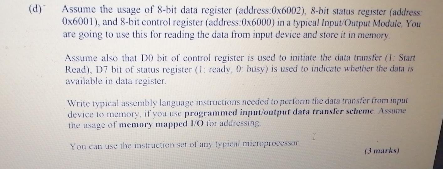
( 6) Assume that 16-bit datal in hexadecimal format is (#0x457F) and 16-bit data2 in hexadecimal format is (#OxAB36). Answer the following: i) Assume the usage of 16-bit Intel 8086 microprocessor, identify the flag bits (carry, overflow, zero, sign, parity) and AX register contents at the end of execution of the following instructions. MOV AX, #0x457F MOV BX,#OXAB36 ADD AX, BX ii) Assume the usage of 32-bit ARM microprocessor, identify the user flag bits (Negative, Zero, Carry) and R3 register contents at the end of execution of the following instructions. I MOV RI, #0x457F MOV R2, #OXAB36 SUBS R3, R1, R2 (3+2 = 5 marks/ Continued... (a) Assume the usage of 5-stage instruction pipelining Instruction Fetch (IF), Instruction Decode (ID), Execute (EX), Memory (MEM), Write Back (WB) with a program consisting of 1000 instructions. Assume that clock cycle per instruction is 1 time unit. Answer the following: i) Assume the usage of ideal pipelining without any hazards, how many time units will be needed to complete all the 1000 instructions. (1 mark) ii) If pipelining is not used, how many time units will be required to execute these 1000 instructions (1 mark) 111) What is the speedup factor on the usage of pipelining for these 1000 instructions (1 mark) (b) Identify the type of data hazard possible in the following instructions in a hypothetical computer and explain the reason I ADD R2RI.R3 SUB R1 R2 RI (2 marks) bunaitheal sampuler (c) Assume that the following instruction has to be executed in a hypothetical computer. SUB R1, [X] X is a indirect memory address which contains the address of data. This instruction is available in memory location Y. Identify the microoperations required to execute this instruction, involving fetch cycle. indirect cycle and execute cycle. (3 marks) (d) Assume that in a multiprocessing environment, data X is available in main memory. If this data is brought into local cache memory of three processors (PL.P2.P3), briefly explain how the cache coherence problem can occur with an illustration (2 marks) 1 Continued... Page 4 of 6 (a) The following arithmetic expression has to be evaluated. H = [D-(B+C))]/[(E*F)-G] Assume that you cannot use B, C, D, E, F, G for storing the results of an instruction. You can use temporary registers R1, R2. Write an assembly language program for a hypothetical computer using (ii) Three-address instructions One-address instructions Zero-address instructions (3 marks) The instructions available for use are as follows: Three address One address LOAD X I ADD XYZ STOREX SUB XYZ ADD N MUL X Y Z SUB DIVYZ VUL DI MUL X,Y SUB X DIV X, Y, Z MUL X DIV X Symbolic Representation and interpretation for n-address instructions are given below. Number of Addresses Symbolic Representation OP A.B.C Interpretation - 3 2 OP A.B - 1 OPA - 0 OP T - ( TD OPT = accumulator T = top of stack = second element of stack A.B.C = memory or register locations Continuel... I Page 5 of 6 STUDENT ID (b) A hypothetical computer system has a hierarchical memory architecture consists of cache memory of size 32 KB with a block size of 32 bytes. CPU generates 32-bit physical addresses Identify the address structures for the following cache memory mapping functions Direct Mapping (No. of bits required for Tag, Line and Word fields) (ii) Eight-way Set Associative Mapping (No. of bits required for Tag, Set, and Word fields) (2 marks) Construct 12-bit Hamming Code for the 8-bit data word 10110101 Show all the steps involved (2 marks) (d) Assume the usage of 8-bit data register (address:0x6002), 8-bit status register (address: 0x6001), and 8-bit control register (address:0x6000) in a typical Input/Output Module. You are going to use this for reading the data from input device and store it in memory. Assume also that Do bit of control register is used to initiate the data transfer (1: Start Read), D7 bit of status register (1: ready, 0: busy) is used to indicate whether the data is available in data register. Write typical assembly language instructions needed to perform the data transfer from input device to memory, if you use programmed input/output data transfer scheme Assume the usage of memory mapped I/O for addressing. You can use the instruction set of any typical microprocessor
Step by Step Solution
There are 3 Steps involved in it

Get step-by-step solutions from verified subject matter experts


