Question
A 6T SRAM cell is fabricated in a 0.13-um CMOS process for which Dp = 1.2 V, V, = 0.4 V, and H,Cor =

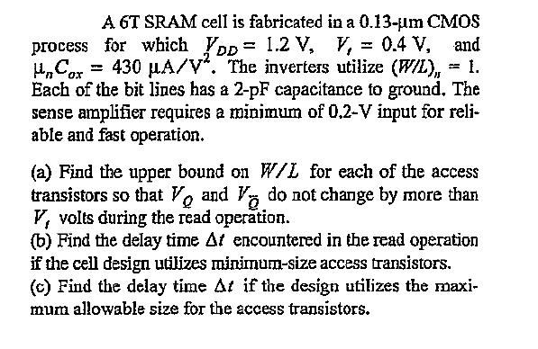
A 6T SRAM cell is fabricated in a 0.13-um CMOS process for which Dp = 1.2 V, V, = 0.4 V, and H,Cor = 430 uA/V*. The inverters utilize (WIL), = 1. Each of the bit lines has a 2-pF capacitance to ground, The sense amplifier requires a minimum of 0.2-V input for reli- able and fast operation. %3D %3! (a) Find the upper bound on WIL for each of the access transistors so that Vo and Vz do not change by more than V, volts during the read operation. (b) Find the delay time Af encountered in the read operation if the cell design utilizes minimum-size access transistors. (c) Find the delay time At if the design utilizes the maxi- mum allowable size for the access transistors.
Step by Step Solution
3.53 Rating (163 Votes )
There are 3 Steps involved in it
Step: 1

Get Instant Access to Expert-Tailored Solutions
See step-by-step solutions with expert insights and AI powered tools for academic success
Step: 2

Step: 3

Ace Your Homework with AI
Get the answers you need in no time with our AI-driven, step-by-step assistance
Get StartedRecommended Textbook for
Probability And Statistics For Engineers And Scientists
Authors: Anthony Hayter
3rd Edition
495107573, 978-0495107576
Students also viewed these Electrical Engineering questions
Question
Answered: 1 week ago
Question
Answered: 1 week ago
Question
Answered: 1 week ago
Question
Answered: 1 week ago
Question
Answered: 1 week ago
Question
Answered: 1 week ago
Question
Answered: 1 week ago
Question
Answered: 1 week ago
Question
Answered: 1 week ago
Question
Answered: 1 week ago
Question
Answered: 1 week ago
Question
Answered: 1 week ago
Question
Answered: 1 week ago
Question
Answered: 1 week ago
Question
Answered: 1 week ago
Question
Answered: 1 week ago
Question
Answered: 1 week ago
Question
Answered: 1 week ago
Question
Answered: 1 week ago
Question
Answered: 1 week ago
Question
Answered: 1 week ago
View Answer in SolutionInn App


