Question
a) Draw the schematic of the 3-input NOR gate, and size all the transistors such that the worst-case delay is equal to that of

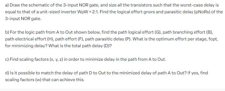
a) Draw the schematic of the 3-input NOR gate, and size all the transistors such that the worst-case delay is equal to that of a unit-sized inverter WpW = 2:1. Find the logical effort gnors and parasitic delay (pNoRs) of the 3-input NOR gate. b) For the logic path from A to Out shown below, find the path logical effort (G), path branching effort (B), path electrical effort (H), path effort (F), path parasitic delay (P). What is the optimum effort per stage, fopt, for minimizing delay? What is the total path delay (D)? c) Find scaling factors (x, y, z) in order to minimize delay in the path from A to Out. d) Is it possible to match the delay of path D to Out to the minimized delay of path A to Out? If yes, find scaling factors (w) that can achieve this.
Step by Step Solution
3.29 Rating (155 Votes )
There are 3 Steps involved in it
Step: 1

Get Instant Access to Expert-Tailored Solutions
See step-by-step solutions with expert insights and AI powered tools for academic success
Step: 2

Step: 3

Ace Your Homework with AI
Get the answers you need in no time with our AI-driven, step-by-step assistance
Get StartedRecommended Textbook for
Analysis and Design of Analog Integrated Circuits
Authors: Paul R. Gray, Paul J. Hurst Stephen H. Lewis, Robert G. Meyer
5th edition
1111827052, 1285401107, 9781285401102 , 978-0470245996
Students also viewed these Electrical Engineering questions
Question
Answered: 1 week ago
Question
Answered: 1 week ago
Question
Answered: 1 week ago
Question
Answered: 1 week ago
Question
Answered: 1 week ago
Question
Answered: 1 week ago
Question
Answered: 1 week ago
Question
Answered: 1 week ago
Question
Answered: 1 week ago
Question
Answered: 1 week ago
Question
Answered: 1 week ago
Question
Answered: 1 week ago
Question
Answered: 1 week ago
Question
Answered: 1 week ago
Question
Answered: 1 week ago
Question
Answered: 1 week ago
Question
Answered: 1 week ago
Question
Answered: 1 week ago
Question
Answered: 1 week ago
Question
Answered: 1 week ago
Question
Answered: 1 week ago
View Answer in SolutionInn App


