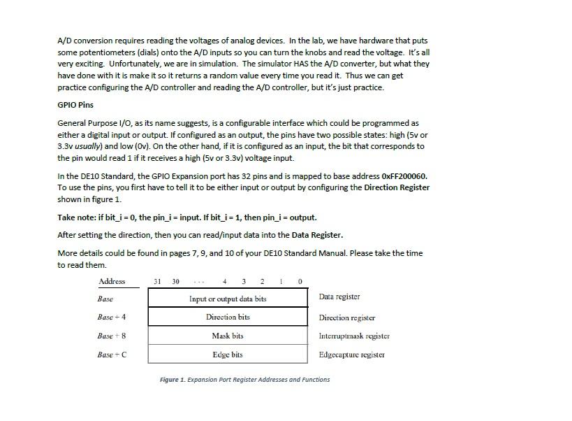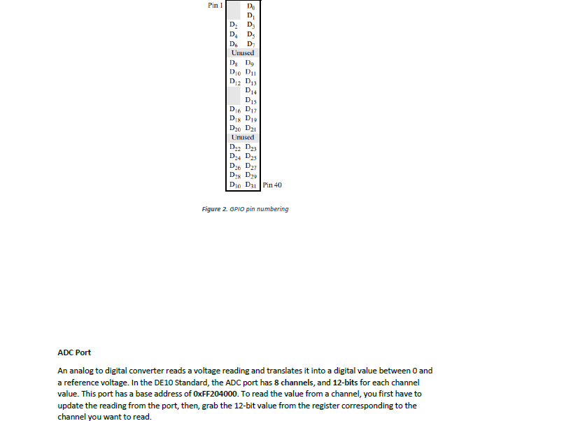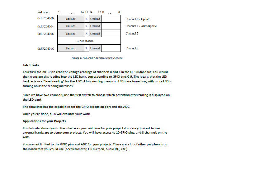


A/D conversion requires reading the voltages of analog devices. In the lab, we have hardware that puts some potentiometers (dials) onto the A/D inputs so you can turn the knobs and read the voltage. It's all very exciting. Unfortunately, we are in simulation. The simulator HAS the A/D converter, but what they have done with it is make it so it returns a random value every time you read it. Thus we can get practice configuring the A/D controller and reading the A/D controller, but it's just practice. GPIO Pins General Purpose I/O, as its name suggests, is a configurable interface which could be programmed as either a digital input or output. If configured as an output, the pins have two possible states: high (5v or 3.3v usually) and low (Ov). On the other hand, if it is configured as an input, the bit that corresponds to the pin would read 1 if it receives a high (5v or 3.3v) voltage input. In the DE10 Standard, the GPIO Expansion port has 32 pins and is mapped to base address OxFF200060. To use the pins, you first have to tell it to be either input or output by configuring the Direction Register shown in figure 1. Take note: if bit_i = 0, the pin_i=input. If bit_i=1, then pin_i = output. After setting the direction, then you can read/input data into the Data Register. More details could be found in pages 7,9, and 10 of your DE10 Standard Manual. Please take the time to read them. Address Input or output data bits Data register Direction bits Direction register Mask bits Interruptmask register Base + c Edge bits Edgecapture register 31 30 0 Base Base +4 Base + 8 Figure 1. Expansion Port Register Addresses and Functions Pin 1 D D D D D D D Unused D D DO DI D2 013 D14 DIS D6 D12 D D 19 D20 021 Unused D.2 D23 D24 D25 D26 27 Dig Dz9 D30 D31 Pin 40 Figure 2 GPIO pin numbering ADC Port An analog to digital converter reads a voltage reading and translates it into a digital value between 0 and a reference voltage. In the DE 10 Standard, the ADC port has 8 channels, and 12-bits for each channel value. This port has a base address of OxFF204000. To read the value from a channel, you first have to update the reading from the port, then, grab the 12-bit value from the register corresponding to the channel you want to read. Address 31 16 15 14 12 11 OxFF 204000 Unused R Unused Channel 0/Update OxFF204004 Unused R Unused Channel 1/Auto-update OxFF204008 Unused Unused Channel 2 ... not shown OxFF204010 Unused Unused Channel 7 Figure 3. ADC Port Addresses and Functions Lab 3 Tasks Your task for lab 3 is to read the voltage readings of channels and 1 in the DE 10 Standard. You would then translate this reading into the LED bank, corresponding to GPIO pins 0-9. The idea is that the LED bank acts as a "level reading for the ADC. A low reading means no LED's are turned on, with more LED's turning on as the reading increases. Since we have two channels, use the first switch to choose which potentiometer reading is displayed on the LED bank. The simulator has the capabilities for the GPIO expansion port and the ADC. Once you're done, a TA will evaluate your work. Applications for your Projects This lab introduces you to the interfaces you could use for your project if in case you want to use external hardware to demo your projects. You will have access to 10 GPIO pins, and 8 channels on the ADC. You are not limited to the GPIO pins and ADC for your projects. There are a lot of other peripherals on the board that you could use (Accelerometer, LCD Screen, Audio 1/0, etc.). A/D conversion requires reading the voltages of analog devices. In the lab, we have hardware that puts some potentiometers (dials) onto the A/D inputs so you can turn the knobs and read the voltage. It's all very exciting. Unfortunately, we are in simulation. The simulator HAS the A/D converter, but what they have done with it is make it so it returns a random value every time you read it. Thus we can get practice configuring the A/D controller and reading the A/D controller, but it's just practice. GPIO Pins General Purpose I/O, as its name suggests, is a configurable interface which could be programmed as either a digital input or output. If configured as an output, the pins have two possible states: high (5v or 3.3v usually) and low (Ov). On the other hand, if it is configured as an input, the bit that corresponds to the pin would read 1 if it receives a high (5v or 3.3v) voltage input. In the DE10 Standard, the GPIO Expansion port has 32 pins and is mapped to base address OxFF200060. To use the pins, you first have to tell it to be either input or output by configuring the Direction Register shown in figure 1. Take note: if bit_i = 0, the pin_i=input. If bit_i=1, then pin_i = output. After setting the direction, then you can read/input data into the Data Register. More details could be found in pages 7,9, and 10 of your DE10 Standard Manual. Please take the time to read them. Address Input or output data bits Data register Direction bits Direction register Mask bits Interruptmask register Base + c Edge bits Edgecapture register 31 30 0 Base Base +4 Base + 8 Figure 1. Expansion Port Register Addresses and Functions Pin 1 D D D D D D D Unused D D DO DI D2 013 D14 DIS D6 D12 D D 19 D20 021 Unused D.2 D23 D24 D25 D26 27 Dig Dz9 D30 D31 Pin 40 Figure 2 GPIO pin numbering ADC Port An analog to digital converter reads a voltage reading and translates it into a digital value between 0 and a reference voltage. In the DE 10 Standard, the ADC port has 8 channels, and 12-bits for each channel value. This port has a base address of OxFF204000. To read the value from a channel, you first have to update the reading from the port, then, grab the 12-bit value from the register corresponding to the channel you want to read. Address 31 16 15 14 12 11 OxFF 204000 Unused R Unused Channel 0/Update OxFF204004 Unused R Unused Channel 1/Auto-update OxFF204008 Unused Unused Channel 2 ... not shown OxFF204010 Unused Unused Channel 7 Figure 3. ADC Port Addresses and Functions Lab 3 Tasks Your task for lab 3 is to read the voltage readings of channels and 1 in the DE 10 Standard. You would then translate this reading into the LED bank, corresponding to GPIO pins 0-9. The idea is that the LED bank acts as a "level reading for the ADC. A low reading means no LED's are turned on, with more LED's turning on as the reading increases. Since we have two channels, use the first switch to choose which potentiometer reading is displayed on the LED bank. The simulator has the capabilities for the GPIO expansion port and the ADC. Once you're done, a TA will evaluate your work. Applications for your Projects This lab introduces you to the interfaces you could use for your project if in case you want to use external hardware to demo your projects. You will have access to 10 GPIO pins, and 8 channels on the ADC. You are not limited to the GPIO pins and ADC for your projects. There are a lot of other peripherals on the board that you could use (Accelerometer, LCD Screen, Audio 1/0, etc.)
