

Answered step by step
Verified Expert Solution
Question
1 Approved Answer
ANSWER USING DIAGRAM AND truth table Boolean Algebra Lab - Part I Activity Overview For this lab we will be using a website called logic.ly
ANSWER USING DIAGRAM AND truth table
Boolean Algebra Lab Part I
Activity Overview
For this lab we will be using a website called
logic.ly This site is designed to allow anyone to use logic gates to build circuits. Though there is a for pay option, we will not be using it for our lab. We will take advantage of their free offerings.
The
logic.ly site has several control panels on the left side of the screen that are of interest and use to us The first is the input panel. There, we will find toggle switches, which will be our basic inputoutput You can experiment with circuits to determine which position allows the switch to be considered on Then there is the output control panel. We will be using the light bulb for our output, however you are free to play and experiment with the other option. Finally, there is also a logic gates panel, which contains all the basic gates we will use and some we will not use See the snips of these panels below. Drag and drop the desired component onto the drawing grid, use your mouse to click on a connection dot and draw a line to the point of the next component you wish to connect to
Figure : Input Control Panel from
logic.ly
Figure : Output Control Panel from
logic.ly
Figure : Logic Gates Panel from
logic.ly
To read the output of a circuit, the light will glow if the output of the whole circuit is true, and will be unlit if it is false. The intermediate steps will be blue if they are true. See the figures below.
Figure : Example AND Gate with all Connections False from
logic.ly
CNIT Intro Computer Architecture Boolean Algebra Lab
Figure : Example AND Gate with One True Input Line from
logic.ly
Important Note: We differentiate between logic gates and the peripheral building components input and output components When tasked with building a circuit using, for example, no more than two logic gate components, you can use two toggle switches, a light output, etc., but only two logic gates AND OR or NOT
Three Input OR
A threeinput OR gate is much like a twoinput version, except it determines whether any one of three input values is true or not. As a single entity it can be illustrated as a single OR gate with three input lines and a single output line see below It can also be illustrated as a circuit of two individual OR gates. Using only twoinput logic gates, build the threeinput OR gate and draw its truth table.
Figure : Three Input OR Symbol
With your lab report, submit the labeled truth table and a labeled snip of your completed logic block circuit. Each figure in this document demonstrates how to label images appropriately. If you do not label your images properly, there will be no assumptions made about what you "intend" to communicate with the image. Without an image label, many questions will receive zero points of credit. This is important now, and in future labs.
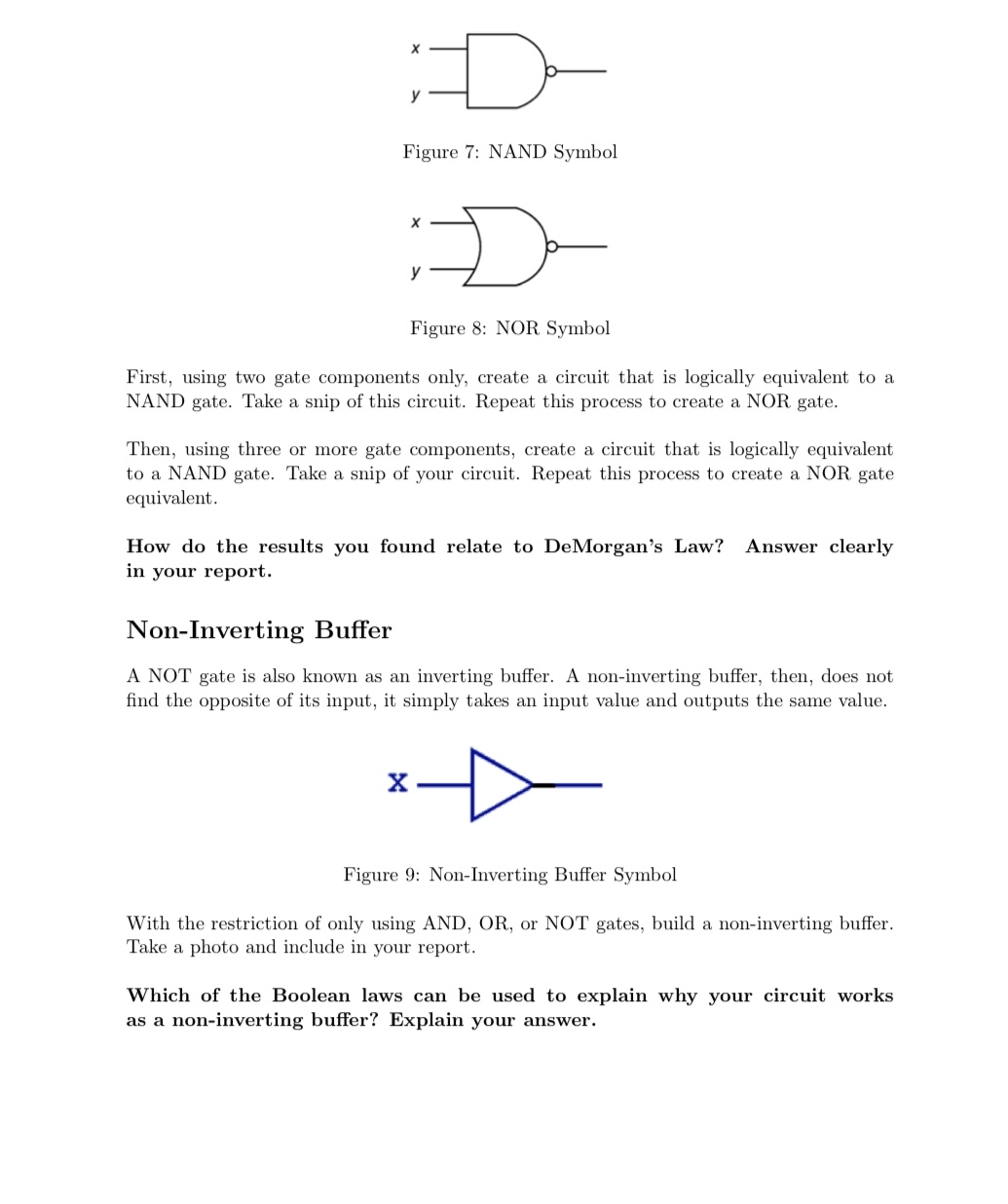
NAND & NOR
In our lecture notes, we see that there is a way to construct all the logic gates using only NAND and NOR gates. However, imagine that our logic block panel only contains AND, OR and NOT gates. Can we do the opposite of constructing everything from NAND and NOR gates and construct NAND and NOR gates using the others?
Figure : NAND Symbol
Figure : NOR Symbol
First, using two gate components only, create a circuit that is logically equivalent to a NAND gate. Take a snip of this circuit. Repeat this process to create a NOR gate.
Then, using three or more gate components, create a circuit that is logically equivalent to a NAND gate. Take a snip of your circuit. Repeat this process to create a NOR gate equivalent.
How do the results you found relate to DeMorgan's Law? Answer clearly in your report.
NonInverting Buffer
A NOT gate is also known as an inverting buffer. A noninverting buffer, then, does not find the opposite of its input, it simply takes an input value and outputs the same value.
Figure : NonInverting Buffer Symbol
With the restriction of only using AND, OR or NOT gates, build a noninverting buffer. Take a photo and include in your report.
Which of the Boolean laws can be used to explain why your circuit works as a noninverting buffer? Explain your answer.
Step by Step Solution
There are 3 Steps involved in it
Step: 1

Get Instant Access to Expert-Tailored Solutions
See step-by-step solutions with expert insights and AI powered tools for academic success
Step: 2

Step: 3
Ace Your Homework with AI
Get the answers you need in no time with our AI-driven, step-by-step assistance
Get Started
Machine Learning And Knowledge Discovery In Databases European Conference Ecml Pkdd 2016 Riva Del Garda Italy September 19 23 2016 Proceedings Part 3 Lnai 9853
Authors: Bettina Berendt ,Bjorn Bringmann ,Elisa Fromont ,Gemma Garriga ,Pauli Miettinen ,Nikolaj Tatti ,Volker Tresp
1st Edition
3319461303, 978-3319461304