Answered step by step
Verified Expert Solution
Question
1 Approved Answer
b ) ? b a r ( R D ) and ? b a r ( M E M R Q ) are control lines
b and are control lines from the CPU. What must their
logic state be in order to read the switches?
This question refers to the CMX CPU, details of which
accompany this assignment.
a With reference to the block diagram of the CPU, what is the
purpose of the program stack and the accumulators and
b Again with reference to the block diagram, outline how the
processor would add two numbers held in ACC.A and ACC.B
the result being stored in memory.
Identify the addressing modes that would be employed in this
addition.
c Give the address range in hex that the PC could access.
Three widely used but different processors are Intel, ARM
and Atmel's AVR.
Identify commonalities and contrast the architecture of these
processors and how this relates to their particular application niche.
a Describe the modes of operation of the Intel Programmable
Peripheral Interface.
b The ASCII bit code for is Express this as bit
evenparity code where the parity bit is the least significant.
cAPCD UART has a clock running at MHz and its
baud rate is set to Determine the HEX contents of its DLM and
DLL registers.
d Using the grid below, sketch a waveform to show how the data
would be transmitted to line using Nonreturntozero
inverted NRZI line encoding. Assume the signal level is initially
high as shown.
a The diagram below shows the structure of a USB token packet.
Identify the function of each field
b Identify the four basic types of data transfers that are supported
by the USB architecture. Write a sentence on how each type is
used
c Identify which OSI model layers are relevant to both USB and
USB
d Outline three improvements offered by USB compated to
USBProgrammer's Model
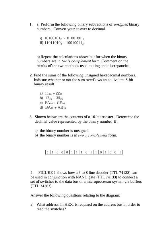
Block Diagramsa Perform the following binary subtractions of unsigned binary
numbers. Convert your answer to decimal.
i
ii
b Repeat the calculations above but for when the binary
numbers are in two's complement form. Comment on the
results of the two methods used, noting and discrepancies.
Find the sums of the following unsigned hexadecimal numbers.
Indicate whether or not the sum overflows an equivalent bit
binary result.
a
b
c
d
Shown below are the contents of a bit resister. Determine the
decimal value represented by the binary number if:
a the binary number is unsigned
b the binary number is in two's complement form.
FIGURE shows how a to line decoder TTL can
be used in conjunction with NAND gate TTL to connect a
set of switches to the data bus of a microprocessor system via buffers
TTL
Answer the following questions relating to the diagram:
a What address, in HEX, is required on the address bus in order to
read the switches?

Step by Step Solution
There are 3 Steps involved in it
Step: 1

Get Instant Access to Expert-Tailored Solutions
See step-by-step solutions with expert insights and AI powered tools for academic success
Step: 2

Step: 3

Ace Your Homework with AI
Get the answers you need in no time with our AI-driven, step-by-step assistance
Get Started


