

Question: Can someone help me with this Digital technology task? Lab 1 - Introduction to Quartus Introduction In this assignment, we will get to know Quartus
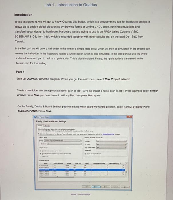
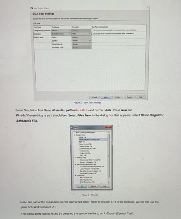
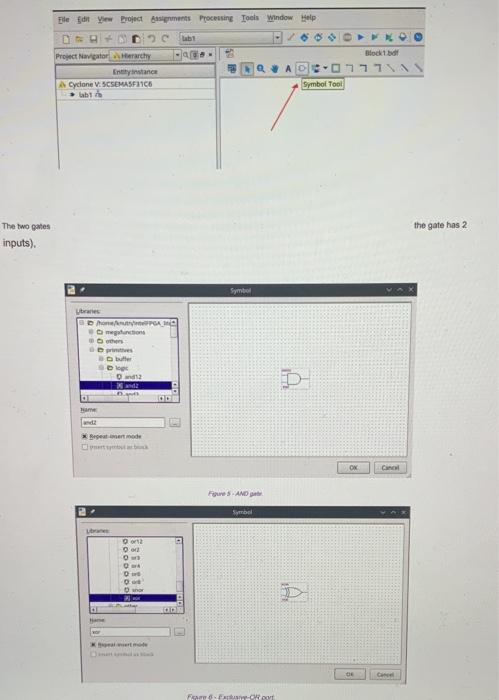
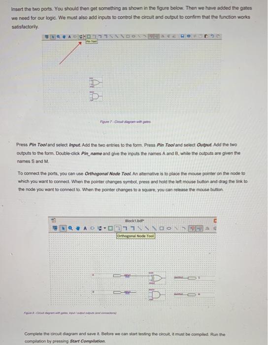
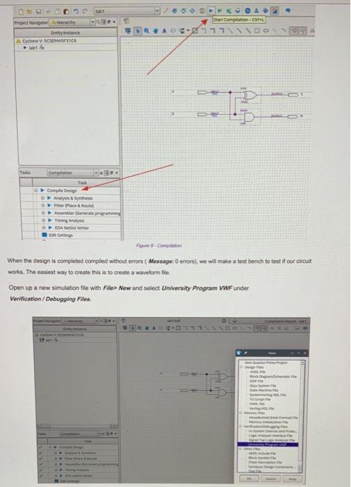
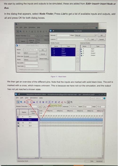
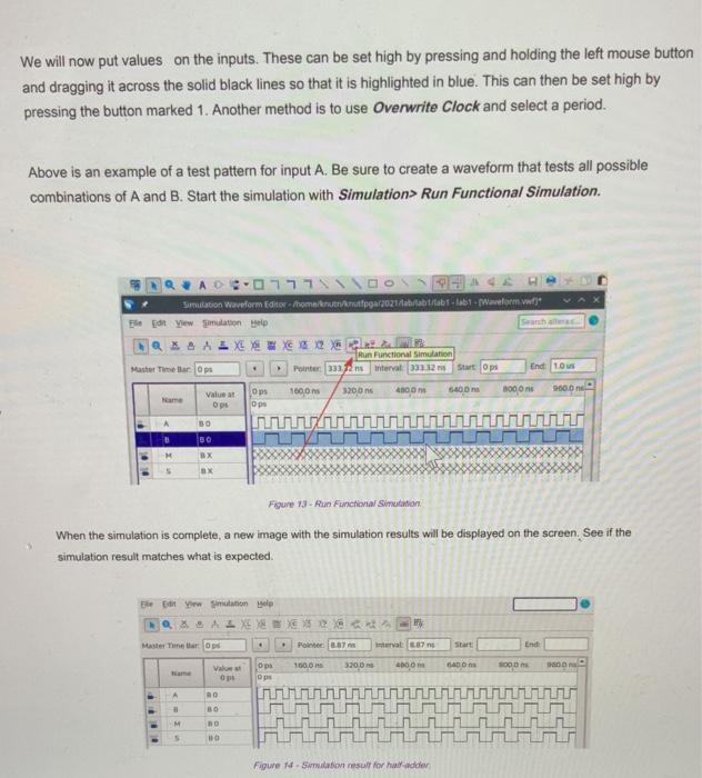
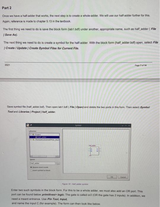
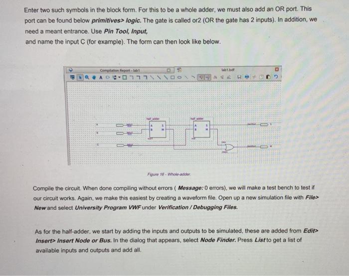
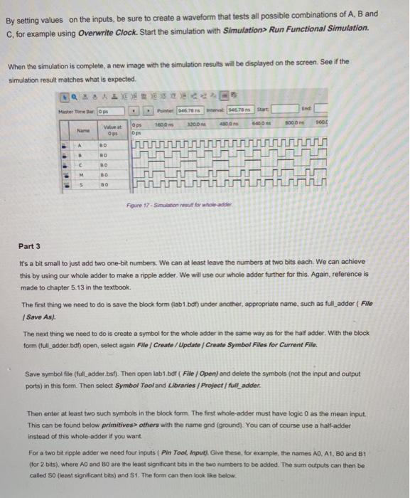
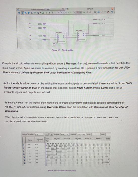
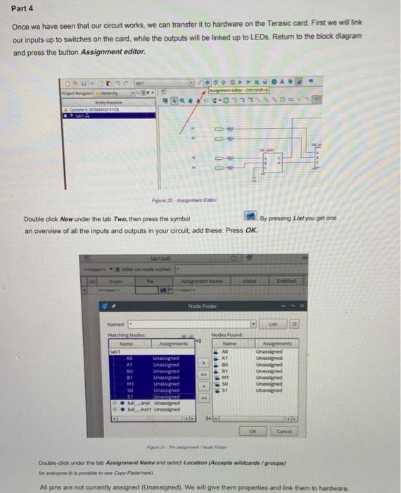
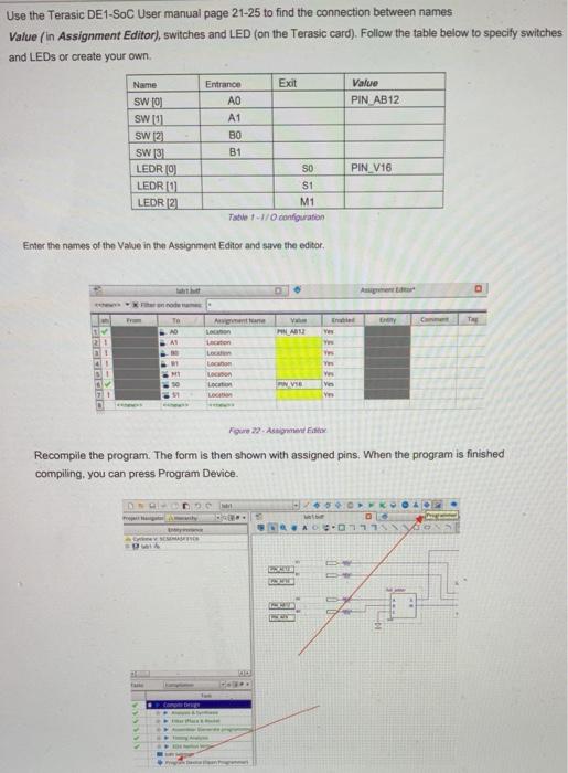
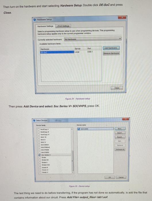
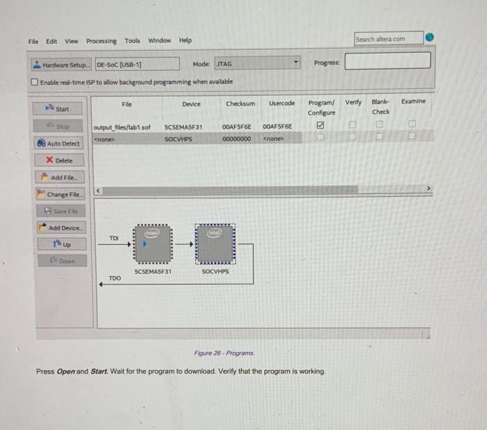
Lab 1 - Introduction to Quartus Introduction In this assignment, we will get to know Quartus Lite better, which is a programming tool for hardware design. It allows us to design digital electronics by drawing forms or writing VHDL code, running simulations and transferring our design to hardware Hardware we are going to use is an FPGA called Cyclone V SOC 5CSEMA5F31C6, from Intel, which is mounted together with other circuits etc. on the card De 1-SOC from Terasic In the first part we will draw a half-adder in the form of a simple logic circuit which will then be simulated. In the second part we use the hail-adder in the first part to realize a whole-addet, which is also simulated. In the third part we use the whole adder in the second part to realize a nipple adder. This is also simulated. Finally, the ripple adder is transferred to the Terasic card for final testing Part 1 Start up Quartus Prime the program. When you get the main menu, select New Project Wizard. Create a new folder with an appropriate name, such as lab1Give the project a name, such as tab1. Press Next and select Empty project, Press Next, you do not want to add any files, then press Next again, On the Family, Device & Board Settings page we set up which board we want to program, select Family: Cyclone V and 5CSEMA5F31C6, Press Next Family, Device & Board Settings See ALME Con LIV CA Gece 314 DIA SCH Foto EDA Tool Settings The Figure 2 - EDA Tools Select Simulation Tool Name ModelSim (-Altera for 18.1 ) and Format VHDL Press Next and Finish (if everything is as it should be). Select File> New, in the dialog box that appears, select Block Diagram/ Schematic File ward - Desy SOLT Tur VOLT VOLI www. VW F3-N In the first part of the assignment we will draw a half-adder. Refer to chapter 5.13 in the textbook. We will first use the gates AND and Exclusive OR. The logical porta can be found by pressing the symbol similar to an AND port (Symbol Tool). File Yew Project Bass Processing Tools Window telp C ab1 Block \ \ Project Navigatory Einsan A Cyclone V. SCSEMASF2106 ht Symbol Tool the gate has 2 The two gates inputs). res DGA glucions 12 D * Beenmode ON Can Four SAND Simbol 12 0:00 D Farve- Insert the two ports. You should then get something as shown in the figure below. Then we have added the gates we need for our logic. We must also add inputs to control the circuit and output to confirm that the function works satisfactorily HOTSTOONS Far na pate Press Pin Tool and select Input. Add the two entries to the form. Press Pin Tool and select Output. Add the two outputs to the form. Double-click Pin_name and give the inputs the names A and B while the outputs are given the names S and M To connect the ports, you can use Orthogonal Node Tool. An alternative is to place the mouse pointer on the node to which you want to connect. When the pointer changes symbol, press and hold the left mouse button and drag the link to the node you want to connect to. When the pointer changes to a square, you can release the mouse button Block1 bdt - \\ Orthogonal Node Tool Complete the circuit diagram and save it. Before we can start testing the circuit, it must be compiled Run the compilation by pressing Start Compilation. lat Prahy Ent dona V. SCSEMASA Seart Citation - Colt AO 02771 D Companion Come Design Analyse Am Genpro - Twin My DAN W When the design is completed compiled without errors Message:0 errors), we will make a test bench to test if our circuit works. The easiest way to create this is to create a waveform file Open up a new simulation file with Files New and select University Program WF under Verification / Debugging Files CH . We start by adding the inputs and outputs to be simulated these are added from Edit> Insert> Insert Node or Bus. In the dialog that appears, select Node Finder, Press List to get a list of available inputs and outputs, add all and press OK for both dialog boxes. DE Cance 0 Se Nos OK UT ry Sarto FIT Mode We then get an overview of the different pins. Note that the inputs are marked with solid black lines. The exit is marked with a cross, which means unknown. This is because we have not run the simulation, and the output has not yet reached a known state. Simon Waveform Edit En View top X X X Master Time BDIA De Clock 17. Sampe End 10 1000 3200 Op Op OD GOO Nane 800 WOO va Ops 30 BO og od We will now put values on the inputs. These can be set high by pressing and holding the left mouse button and dragging it across the solid black lines so that it is highlighted in blue. This can then be set high by pressing the button marked 1. Another method is to use Overwrite Clock and select a period. Above is an example of a test pattern for input A. Be sure to create a waveform that tests all possible combinations of A and B. Start the simulation with Simulation> Run Functional Simulation. AD0771 VOOR Simulation Waveform Editorhomarunkag/2021/ab/a/1061 - 1ab1.Waveform wwf]* Flet View imulation help a XA Run Functional Simulation Master in Bars Pointer 33 interval 23.12 Start Ops End: 10 1000 3200 4800 6400 1000 900.0 Ops ops Name Value at 30 un BX BX Figure 13 - Run Functional Simutition When the simulation is complete, a new image with the simulation results will be displayed on the screen See if the simulation result matches what is expected Edit Simulation Help NQ XOAYE VE Master Tear Hinter 87 ms 6.87 End 1000 320,00 11 640 000 Ops pe 00 Vako op A RO BO . M RO 10 Figure 14 Simulation result for hadde Part 2 Once we have a half-adder that works, the next step is to create a whole-adder. We will use our half-adder further for this. Again, reference is made to chapter 5.13 in the textbook The first thing we need to do is save the block form (lab1.bdf) under another, appropriate name, such as half_adder (Fle Save As). The next thing we need to do is create a symbol for the half-adder. With the block form (half_adder bdf) open, select File Create/Update Create Symbol Files for Current File. 2021 Page of 4 Save symbol file (half_adder buf). Then open lab1 bdt ( File / Open) and delete the two ports in this form. Then select Symbol Tool and Libraries / Project / hall_adder. bol ws Manthera to shock tro Enter two such symbols in the block form. For this to be a whole adder, we must also add an OR port. This port can be found below primitives logic. The gate is called 0-2 (OR the gate has 2 inputs). In addition, we need a meant entrance. Use Pin Tool, Input and name the input (for example). The form can then look like below. Enter two such symbols in the block form. For this to be a whole adder, we must also add an OR port. This port can be found below primitives> logic. The gate is called or2 (OR the gate has 2 inputs). In addition, we need a meant entrance. Use Pin Tool, Input, and name the input C (for example). The form can then look like below. Compilation Reportlab Labb 770019A 1 D- Figure 16 Wholesale Compile the circuit. When done compiling without errors ( Message:0 errors), we will make a test bench to test if our circuit works. Again, we make this easiest by creating a waveform file. Open up a new simulation file with File> New and select University Program VWF under Verification / Debugging Files. As for the half-adder, we start by adding the inputs and outputs to be simulated, these are added from Edit Insert> Insert Node or Bus. In the dialog that appears, select Node Finder Press List to get a list of available inputs and outputs and add all. By setting values on the inputs, be sure to create a waveform that tests all possible combinations of A, B and C, for example using Overwrite Clock. Start the simulation with Simulation> Run Functional Simulation. When the simulation is complete, a new image with the simulation results will be displayed on the screen See if the simulation result Matches what is expected XXIX End Master Tears P: 46 ms at Start ops 1600 3200 1800 SOO 3000 1606 Nanna Vaat Ops Or A LOUD 9 999 M . 5 50 Figure 97- Sumatanon result for wholder Part 3 It's a bit small to just add two one-bit numbers. We can at least leave the numbers at two bits each. We can achieve this by using our whole adder to make a ripple adder. We will use our whole adder further for this. Again, reference is made to chapter 5.13 in the textbook. The first thing we need to do is save the block form (lab 1 bdf) under another, appropriate name, such as full_adder (File Save As) The next thing we need to do is create a symbol for the whole adder in the same way as for the half adder. With the block form (full_adder bah) open, select again File Create/Update Create Symbol Files for Current File. Save symbol file (full_adder bsf). Then open lab1.bdt (File Open) and delete the symbols (not the input and output ports) in this form. Then select Symbol Tooland Libraries/Project full adder. Then enter at least two such symbols in the block form. The first whole-adder must have logic O as the mean input. This can be found below primitives others with the name gnd (ground). You can of course use a half-adder instead of this whole-adder if you want For a two bit ripple adder we need four inputs ( Pin Tool, Input). Give these, for example, the names A0, A1, BO and 1 (for 2 bits), where A and B are the least significant bits in the two numbers to be added. The sum outputs can then be called SO (least significant bits) and $1. The form can then look like below. Common Report tabt MOB:0771 INDOSA Figure 18 - Reader Compile the circuit. When done compiling without errors ( Message:0 errors), we need to create a test bench to test if our circuit works. Again, we make this easiest by creating a waveform file. Open up a new simulation file with Files New and select University Program WWF under Verification/Debugging Files. As for the whole adder, we start by adding the inputs and outputs to be simulated, these are added from Edit Insert> Insert Node or Bus. In the dialog that appears, select Node Finder Press List to get a list of available inputs and outputs and add all. By setting values on the inputs, then make sure to create a waveform that tests all possible combinations of AO, BO, A1 and A1, for example using Overwrite Clock. Start the simulation with Simulation> Run Functional Simulation. When the simulation is complete, a new image with the simulation results will be displayed on the screen see if the simulation result matches what is expected. Tuner . PT.1 St 100 10 100 OD ope AD 30 NO H A1 31 HO 50 For adder Part 4 Once we have seen that our circuit works, we can transfer it to hardware on the Terasic card. First we will link our inputs up to switches on the card, while the outputs will be linked up to LEDs. Return to the block diagram and press the button Assignment editor. A. OOO-0171 DO Done VISCERAMIC L Figure 2 And Double click New under the tab Two, then press the symbol By pressing List you get one an overview of all the inputs and outputs in your circuit, add these. Press OK. tabbed Filter on moderne TO Tube 1 Node Finder Named LE Matching Node Nodes Found Assignments tab1 NO A1 . Unasugned AL Unassigned Uued Unsigned MI Unsigned SO Unased 51 fullt Und MIT Unsigned Assements Unassigned Unassigned Used Unsigned Unsigned Unassigned Ured TO GE Double-dick under the tab Assignment Name and select Location (Accepts wildcards/groups) for everyone is possible to use them All pins are not currently assigned (Unassigned). We will give them properties and link them to hardware. Use the Terasic DE 1-SOC User manual page 21-25 to find the connection between names Value (in Assignment Editor), switches and LED (on the Terasic card). Follow the table below to specify switches and LEDs or create your own Value PIN AB12 Name swol SW10 SW12 SW3 LEDRO LEDR 10 LEDR(2) Entrance Exit A1 BO B1 SO S1 M1 Table I/O configuration PIN V16 Enter the names of the value in the Assignment Editor and save the editor Art ABS AD A1 Lo Loc VE Ver Figure 22. Atsime Recompile the program. The form is then shown with assigned pins. When the program is finished compiling, you can press Program Device. DOC DC OLUN Then turn on the hardware and start selecting Hardware Setup Double click DE-SoC and press Close Hardware Setup Hardware Setting ITAG Seng Select a programing hardware up to use when programming devices. This program hardware soplesny to the current program window Currently selected hardware Hardware Avhandweretem Add arwar andwe Server LOG RAH Figure Hardware setup Then press Add Device and select Soc Series > SOCVHPS, press OK. Devi MOVIES mont Devo Het may EN MAX 10 MAX MAN DACIA MAXTOLAE MAX CA x F Device The last thing we need to do before transferring. If the program has not done so automatically, is add the file that contains information about our circuit. Press Add Files output files> lab1.sof. File Edit View Processing Tools Window Help Search altera.com Hardware Setup DE-SOC USB-11 Mode: JTAG Progress Enable real-time ISP to allow background programming when available File Device Checksum Usercode Verify Examine Start Program/ Configure Blank- Check Stop output_files/lab1 sof OOAF5F6E OOAFSF6E 5CSEMASF31 SOCVHPS none 00000000
Step by Step Solution
There are 3 Steps involved in it

Get step-by-step solutions from verified subject matter experts