Answered step by step
Verified Expert Solution
Question
1 Approved Answer
can you please zoom in to questions Which statement about a flip flop (dff) is NOT true? Select one: O a. A dff can be

can you please zoom in to questions
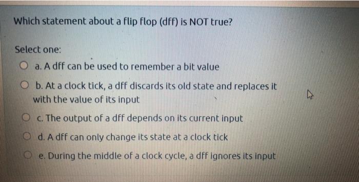
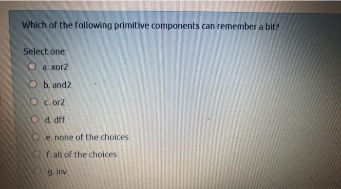
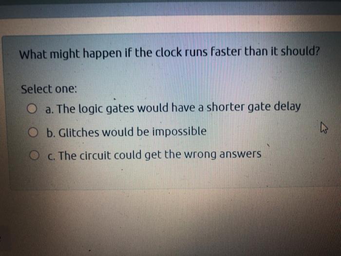
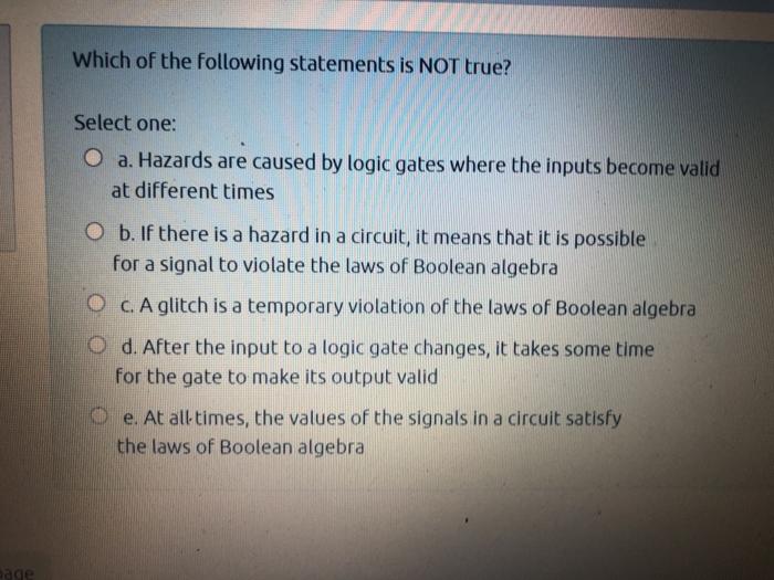
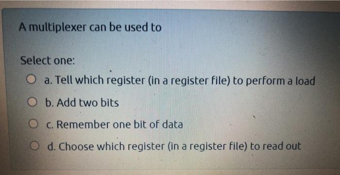
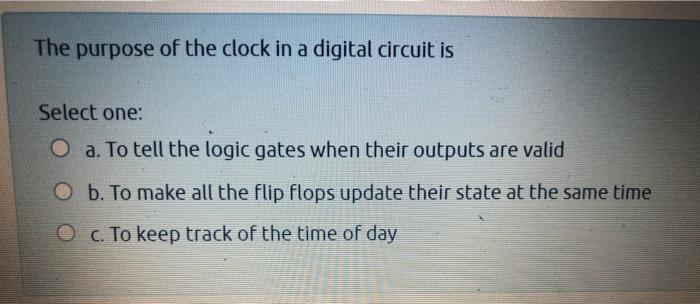
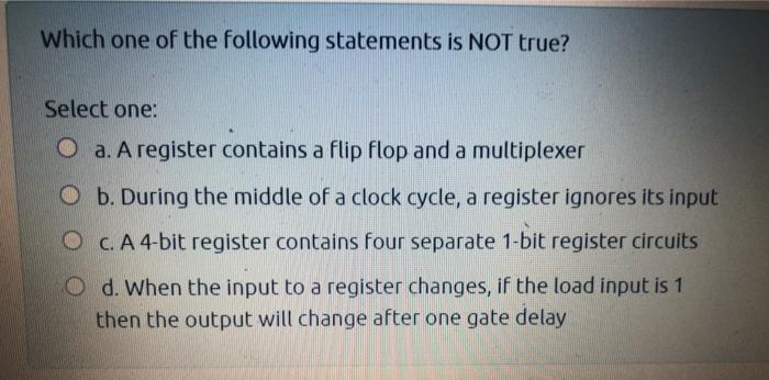
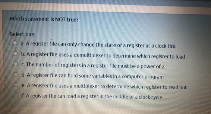
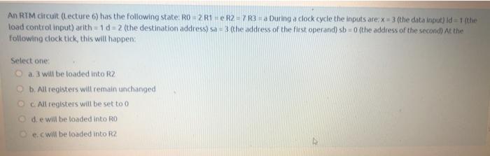
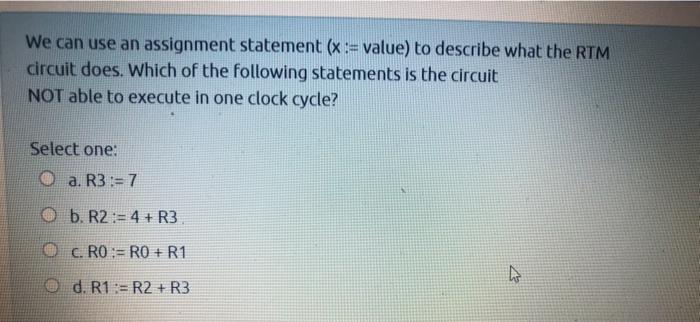
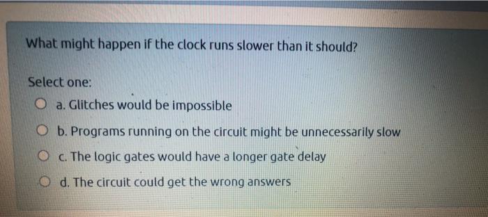
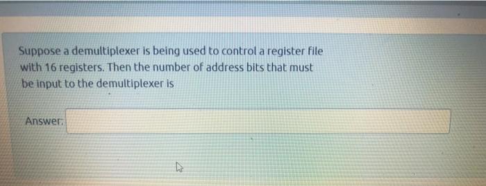
Which statement about a flip flop (dff) is NOT true? Select one: O a. A dff can be used to remember a bit value O b. At a clock tick, a dff discards its old state and replaces it with the value of its input O c. The output of a dff depends on its current input d. A dff can only change its state at a clock tick e. During the middle of a clock cycle, a dff ignores its input Which of the following primitive components can remember a bit? Select one: a. xor2 b. and2 C.or2 d. dff e. none of the choices f. all of the choices g. inv What might happen if the clock runs faster than it should? Select one: O a. The logic gates would have a shorter gate delay O b. Glitches would be impossible C. The circuit could get the wrong answers Which of the following statements is NOT true? Select one: O a. Hazards are caused by logic gates where the inputs become valid at different times O b. If there is a hazard in a circuit, it means that it is possible for a signal to violate the laws of Boolean algebra O c A glitch is a temporary violation of the laws of Boolean algebra O d. After the input to a logic gate changes, it takes some time for the gate to make its output valid e. At all times, the values of the signals in a circuit satisfy the laws of Boolean algebra aage A multiplexer can be used to Select one: O a. Tell which register (in a register file) to perform a load O b. Add two bits O c. Remember one bit of data O d. Choose which register (in a register file) to read out The purpose of the clock in a digital circuit is Select one: O a. To tell the logic gates when their outputs are valid O b. To make all the flip flops update their state at the same time O c. To keep track of the time of day Which one of the following statements is NOT true? Select one: O a. A register contains a flip flop and a multiplexer O b. During the middle of a clock cycle, a register ignores its input O c. A 4-bit register contains four separate 1-bit register circuits O d. When the input to a register changes, if the load input is 1 then the output will change after one gate delay Which statement is NOT true? Select one: O a. A register file can only change the state of a register at a clock tick Ob. A register file uses a demultiplexer to determine which register to load O c. The number of registers in a register file must be a power of 2 d. A register file can hold some variables in a computer program e. A register file uses a multiplexer to determine which register to read out f. A register file can load a register in the middle of a clock cycle An RTM drcuit (lecture 6) has the following state: RO = 2 R1 R2-7R3 - a During a clock cycle the inputs are: x=3 (the data input id=1(the load control input) arith = 10 = 2 (the destination address) sa - 3 (the address of the first operand) sb #0 (the address of the second) At the following clock tick, this will happens Select one O a. 3 will be loaded into R2 b. All registers will remain unchanged All registers will be set to o de will be loaded into RO e will be loaded into R2 An RIM Circuit (l.edure 6) has the following state: RO = 2 R1 = R2 = 7 R3 =a During a cock cycle the inputs are x=3 (the data input) id = 1 (the load control input) arith=0d -2 (the destination address) sa 3 (the address of the first operand) sb = 0 (the address of the second) At the following clock tick, this will happen: Select one: a. 3 will be loaded into R2 o be will be loaded into RO All registers will be set to 0 d. All registers will remain unchanged ec will be loaded into R2 We can use an assignment statement (x:= value) to describe what the RTM circuit does. Which of the following statements is the circuit NOT able to execute in one clock cycle? Select one: a. R3 :=7 b. R2 := 4 + R3 O C. RO := RO + R1 V d. R1 := R2 + R3 What might happen if the clock runs slower than it should? Select one: O a. Glitches would be impossible O b. Programs running on the circuit might be unnecessarily slow O c. The logic gates would have a longer gate delay O d. The circuit could get the wrong answers Suppose a demultiplexer is being used to control a register file with 16 registers. Then the number of address bits that must be input to the demultiplexer is Answer: h Suppose the state of a dff is 1 and its input is 0. When a clock tick occurs, the state becomes Answer: Suppose the state of a dff is 1 and its input is 0, and the circuit is in the middle of a clock cycle. Then the output of the dff is Answer: Suppose a computer program contains the following assignment statement: X=2+3 How many clock cycles would be required to execute this statement on the RTM circuit? (Assume that the registers contain unknown values, and the variable x is in one of the registers.) Answer: The RTM circuit shown in the lectures contains 4 registers, and each register contains a 4-bit word. The total number of Flip flops is Step by Step Solution
There are 3 Steps involved in it
Step: 1

Get Instant Access to Expert-Tailored Solutions
See step-by-step solutions with expert insights and AI powered tools for academic success
Step: 2

Step: 3
Ace Your Homework with AI
Get the answers you need in no time with our AI-driven, step-by-step assistance
Get Started