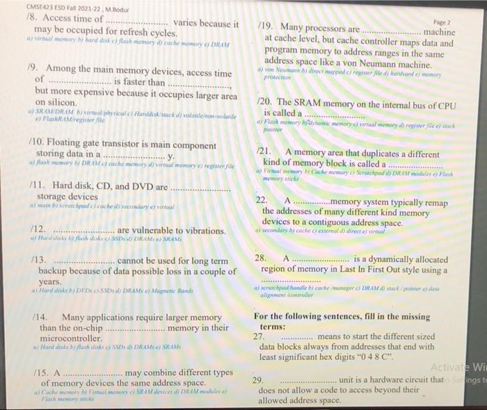
CMSE473 ESD Fall 2021 22 M.Bodur 78. Access time of varies because it may be occupied for refresh cycles. a) Wirtual memory) hard disk a memory drache memory RA Page 2 119. Many processors are machine at cache level, but cache controller maps data and program memory to address ranges in the same address space like a von Neumann machine. 1) von Norman y direct mapped e) register file di hanturde memory protection 20. The SRAM memory on the internal bus of CPU is called a a Plush memory ay namic memory dual memory a register flee) stock poter 19. Among the main memory devices, access time of is faster than but more expensive because it occupies larger area on silicon 4) SREMA DRAMD) Nirmal y vicate) Maridisk Stock / verlatile non-duelle Flandriveste le /10. Floating gate transistor is main component storing data in a ... y. a) Mhesh memory b) DRAMC) che memory daul menary e) rogerie /11. Hard disk, CD, and DVD are storage devices w/ main scratchpads) coche di secondary i wiernaal 21. A memory area that duplicates a different kind of memory block is called a . wiemy Ciche memory Scratchpad / DRAM modules Flash memory stick 22 A ..memory system typically remap the addresses of many different kind memory devices to a contiguous address space. a secondary b) coche el external i directe real /12. are vulnerable to vibrations. w Her SSD) DA SE /13 cannot be used for long term backup because of data possible loss in a couple of years. aitant afisk / DIDCH SSD:4 DRAMG e Mupoetie Hands 28. A is a dynamically allocated region of memory in Last In First Out style using a ay scrutchpaid handle b) cache major SCRAMO stek/pintures de ligner /14 Many applications require larger memory than the on-chip memory in their microcontroller Hand in hand with c) SSD, DRAMRO SRA For the following sentences, fill in the missing terms: 27. ............ means to start the different sized data blocks always from addresses that end with least significant hex digits 0 4 8 CM Activate Wi 29. unit is a hardware circuit thatings to does not allow a code to access beyond their allowed address space 715. A may combine different types of memory devices the same address space. Genital meu SRAM ano d) DRAM es el CMSE473 ESD Fall 2021 22 M.Bodur 78. Access time of varies because it may be occupied for refresh cycles. a) Wirtual memory) hard disk a memory drache memory RA Page 2 119. Many processors are machine at cache level, but cache controller maps data and program memory to address ranges in the same address space like a von Neumann machine. 1) von Norman y direct mapped e) register file di hanturde memory protection 20. The SRAM memory on the internal bus of CPU is called a a Plush memory ay namic memory dual memory a register flee) stock poter 19. Among the main memory devices, access time of is faster than but more expensive because it occupies larger area on silicon 4) SREMA DRAMD) Nirmal y vicate) Maridisk Stock / verlatile non-duelle Flandriveste le /10. Floating gate transistor is main component storing data in a ... y. a) Mhesh memory b) DRAMC) che memory daul menary e) rogerie /11. Hard disk, CD, and DVD are storage devices w/ main scratchpads) coche di secondary i wiernaal 21. A memory area that duplicates a different kind of memory block is called a . wiemy Ciche memory Scratchpad / DRAM modules Flash memory stick 22 A ..memory system typically remap the addresses of many different kind memory devices to a contiguous address space. a secondary b) coche el external i directe real /12. are vulnerable to vibrations. w Her SSD) DA SE /13 cannot be used for long term backup because of data possible loss in a couple of years. aitant afisk / DIDCH SSD:4 DRAMG e Mupoetie Hands 28. A is a dynamically allocated region of memory in Last In First Out style using a ay scrutchpaid handle b) cache major SCRAMO stek/pintures de ligner /14 Many applications require larger memory than the on-chip memory in their microcontroller Hand in hand with c) SSD, DRAMRO SRA For the following sentences, fill in the missing terms: 27. ............ means to start the different sized data blocks always from addresses that end with least significant hex digits 0 4 8 CM Activate Wi 29. unit is a hardware circuit thatings to does not allow a code to access beyond their allowed address space 715. A may combine different types of memory devices the same address space. Genital meu SRAM ano d) DRAM es el


