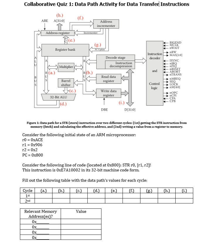
Collaborative Quiz 1: Data Path Activity for Data Transfer Instructions (h.) A[31:01 (1. ABE Address incrementer Incrementer Address register K Te.) #RIGEND nWAIT Register bank NRW Instruction Decode stage L Instruction decompression Multiplier Barrel Read data register Instruction MAS(1:0) decoder ISYNC nIRQ FIO nRFSET and ABORT TRANS nMREQ SEQ. Control LLOCK logic nM[4:0) OPC nCPI CPA CPB shifter (c Write data register 32-Bit ALU (d) (i.) D[31:0) DBE Figure 1: Data path for a STR (store) instruction over two different cycles: (1st) getting the STR instruction from memory (fetch) and calculating the effective address, and (2nd) writing a value from a register to memory. Consider the following initial state of an ARM microprocessor: r0 = OxACE r1 = 0x906 r2 = 0x2 PC = 0x800 Consider the following line of code (located at 0x800): STR 0,[r1, r2]! This instruction is 0xE7A10002 in its 32-bit machine code form. Fill out the following table with the data path's values for each cycle: Cycle (a) (b.) (c) (d) (e) (f) (8.) (h.) (1) 1st 2nd TTTTTTT Value Relevant Memory Address(es)? Ox Ox Ox Collaborative Quiz 1: Data Path Activity for Data Transfer Instructions (h.) A[31:01 (1. ABE Address incrementer Incrementer Address register K Te.) #RIGEND nWAIT Register bank NRW Instruction Decode stage L Instruction decompression Multiplier Barrel Read data register Instruction MAS(1:0) decoder ISYNC nIRQ FIO nRFSET and ABORT TRANS nMREQ SEQ. Control LLOCK logic nM[4:0) OPC nCPI CPA CPB shifter (c Write data register 32-Bit ALU (d) (i.) D[31:0) DBE Figure 1: Data path for a STR (store) instruction over two different cycles: (1st) getting the STR instruction from memory (fetch) and calculating the effective address, and (2nd) writing a value from a register to memory. Consider the following initial state of an ARM microprocessor: r0 = OxACE r1 = 0x906 r2 = 0x2 PC = 0x800 Consider the following line of code (located at 0x800): STR 0,[r1, r2]! This instruction is 0xE7A10002 in its 32-bit machine code form. Fill out the following table with the data path's values for each cycle: Cycle (a) (b.) (c) (d) (e) (f) (8.) (h.) (1) 1st 2nd TTTTTTT Value Relevant Memory Address(es)? Ox Ox Ox


