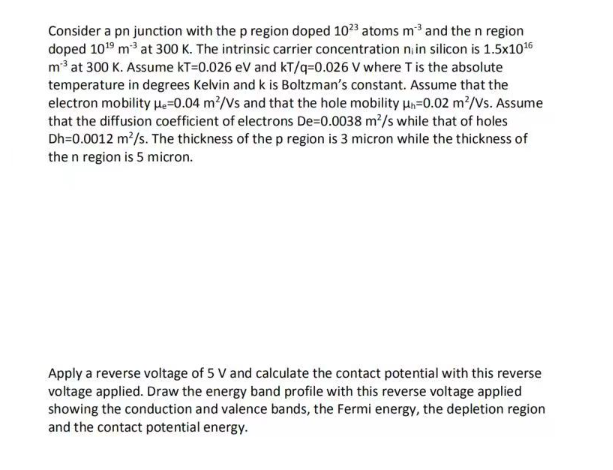
Consider a pn junction with the p region doped 1025 atoms mo and the n region doped 10 m at 300 K. The intrinsic carrier
Consider a pn junction with the p region doped 1025 atoms mo and the n region doped 10" m" at 300 K. The intrinsic carrier concentration min silicon is 1.5x10¹⁶ mos at 300 K. Assume kT=0.026 ev and kT/q=0.026 V where T is the absolute temperature in degrees Kelvin and k is Boltzman's constant. Assume that the electron mobility He=0.04 m /Vs and that the hole mobility un=0.02 m /Vs. Assume that the diffusion coefficient of electrons De=0.0038 m'/s while that of holes Dh=0.0012 m /s. The thickness of the p region is 3 micron while the thickness of the n region is 5 micron. Apply a reverse voltage of 5 V and calculate the contact potential with this reverse voltage applied. Draw the energy band profile with this reverse voltage applied showing the conduction and valence bands, the Fermi energy, the depletion region and the contact potential energy
Step by Step Solution
There are 3 Steps involved in it
Step: 1
Get Instant Access with AI-Powered Solutions
See step-by-step solutions with expert insights and AI powered tools for academic success
Step: 2
Step: 3
Ace Your Homework with AI
Get the answers you need in no time with our AI-driven, step-by-step assistance