Answered step by step
Verified Expert Solution
Question
1 Approved Answer
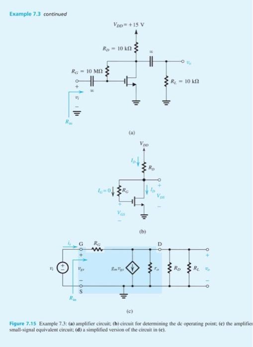
Consider the amplifier circuit of Fig. 7.15(a) without the load resistance R, and with channel-length modulation neglected. Let Vpp = 5 V, V, =


Consider the amplifier circuit of Fig. 7.15(a) without the load resistance R, and with channel-length modulation neglected. Let Vpp = 5 V, V, = 0.7 V, and k = 1 mA/V. Find Vov. I. R. and R, to obtain a voltage gain of -25 V/V and an input resistance of 0.5 M 2. What is the maximum allowable input signal, ? Example 7.3 continued 25 Ra 10 M + 11 Ri 154 105 8- Ra VDD = + 15 V R = 10 kn www 16=0: www 8m + VOD Iv (1 Rp R = 10 kf www www 3 www R % (c) Figure 7.15 Example 7.3: (a) amplifier circuit; (b) circuit for determining the de operating point: (c) the amplifier small-signal equivalent circuit; (d) a simplified version of the circuit in (c).
Step by Step Solution
There are 3 Steps involved in it
Step: 1
V 07 V k 1 mA V V Vgs RG www 8mgs ii RD Design for A V ...
Get Instant Access to Expert-Tailored Solutions
See step-by-step solutions with expert insights and AI powered tools for academic success
Step: 2

Step: 3

Ace Your Homework with AI
Get the answers you need in no time with our AI-driven, step-by-step assistance
Get Started


