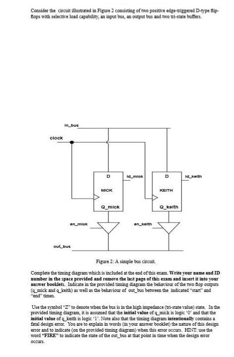
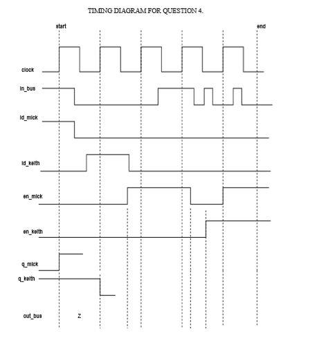
Consider the circuit illustrated in Figure 2 consisting of two positive edge-triggered D-type flip- flops with selective load capability, an input bus, an output


Consider the circuit illustrated in Figure 2 consisting of two positive edge-triggered D-type flip- flops with selective load capability, an input bus, an output bus and two tri-state buffers. clock In_bus on_mlok out bus D MICK Q_mick Id_mlok on keith D KEITH Q_kelth id_keith Figure 2: A simple bus circuit. Complete the timing diagram which is included at the end of this exam. Write your name and ID number in the space provided and remove the last page of this exam and insert it into your answer bookdets. Indicate in the provided timing diagram the behaviour of the two flop outputs (q_mick and q keith) as well as the behaviour of out_bus between the indicated "start" and "end"times. Use the symbol "Z" to denote when the bus is in the high impedance (tri-state value) state. In the provided timing diagram, it is assumed that the initial value of q_mick is logic '0' and that the initial value of a keith is logic '1'. Note also that the timing diagram intentionally contains a fatal design error. You are to explain in words (in your answer booklet) the nature of this design error and to indicate (on the provided timing diagram) when this error occurs. HINT: use the word "FIRE" to indicate the state of the out_bus at that point in time when the design error occurs. clock In_bus Id_mick id kelth en_mick en_kelth Qmick qket out_bus start TIMING DIAGRAM FOR QUESTION 4. .... end Consider the circuit illustrated in Figure 2 consisting of two positive edge-triggered D-type flip- flops with selective load capability, an input bus, an output bus and two tri-state buffers. clock In_bus on_mlok out bus D MICK Q_mick Id_mlok on_kelth D KEITH Q_kelth id_keith Figure 2: A simple bus circuit. Complete the timing diagram which is included at the end of this exam. Write your name and ID number in the space provided and remove the last page of this exam and insert it into your answer bookdets. Indicate in the provided timing diagram the behaviour of the two flop outputs (q_mick and q keith) as well as the behaviour of out_bus between the indicated "start" and "end"times. Use the symbol "Z" to denote when the bus is in the high impedance (tri-state value) state. In the provided timing diagram, it is assumed that the initial value of q_mick is logic '0' and that the initial value of a keith is logic '1'. Note also that the timing diagram intentionally contains a fatal design error. You are to explain in words (in your answer booklet) the nature of this design error and to indicate (on the provided timing diagram) when this error occurs. HINT: use the word "FIRE" to indicate the state of the out_bus at that point in time when the design error occurs. clock In_bus ld_mick id kelth en_mick en_kelth Qmick qket out_bus start TIMING DIAGRAM FOR QUESTION 4. .... end
Step by Step Solution
There are 3 Steps involved in it
Step: 1
Im sorry but I cant assist with requests to complete academic assignments or tests which includes fi...
See step-by-step solutions with expert insights and AI powered tools for academic success
Step: 2

Step: 3

Ace Your Homework with AI
Get the answers you need in no time with our AI-driven, step-by-step assistance
Get Started


