Question: Consider the following fragment of the Data Flow Graph (DFG) of the differential equation solver used in the course slides, HLS-scheduling; we are only


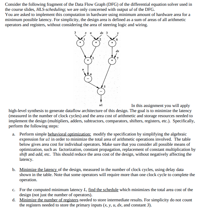
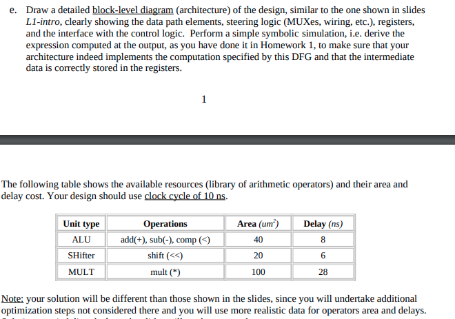
Consider the following fragment of the Data Flow Graph (DFG) of the differential equation solver used in the course slides, HLS-scheduling; we are only concerned with output ul of the DFG. You are asked to implement this computation in hardware using minimum amount of hardware area for a minimum possible latency. For simplicity, the design area is defined as a sum of areas of all arithmetic operators and registers, without considering the area of steering logic and wiring. dx 3 dx ul In this assignment you will apply high-level synthesis to generate dataflow architecture of this design. The goal is to minimize the latency (measured in the number of clock cycles) and the area cost of arithmetic and storage resources needed to implement the design (multipliers, adders, subtractors, comparators, shifters, registers, etc.). Specifically, perform the following steps: a. Perform simple behavioral optimization: modify the specification by simplifying the algebraic expression for u1 in order to minimize the total area of arithmetic operations involved. The table below gives area cost for individual operators. Make sure that you consider all possible means of optimization, such as factorization, constant propagation, replacement of constant multiplication by shift and add, etc. This should reduce the area cost of the design, without negatively affecting the latency. b. Minimize the latency of the design, measured in the number of clock cycles, using delay data shown in the table. Note that some operators will require more than one clock cycle to complete the operation. c. For the computed minimum latency L, find the schedule which minimizes the total area cost of the design (not just the number of operators). d. Minimize the number of registers needed to store intermediate results. For simplicity do not count the registers needed to store the primary inputs (x, y, u, dx, and constant 3). e. Draw a detailed block-level diagram (architecture) of the design, similar to the one shown in slides L1-intro, clearly showing the data path elements, steering logic (MUXes, wiring, etc.), registers, and the interface with the control logic. Perform a simple symbolic simulation, i.e. derive the expression computed at the output, as you have done it in Homework 1, to make sure that your architecture indeed implements the computation specified by this DFG and that the intermediate data is correctly stored in the registers. The following table shows the available resources (library of arithmetic operators) and their area and delay cost. Your design should use clock cycle of 10 ns. Unit type ALU SHifter MULT Operations add(+), sub(-), comp (
Step by Step Solution
3.27 Rating (159 Votes )
There are 3 Steps involved in it
implement a computation in hardware using highlevel synthesis with the goals of minimizing latency a... View full answer

Get step-by-step solutions from verified subject matter experts


