

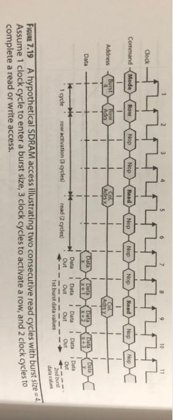
Question
Consider the SDRAM timing diagram in Figure 7.19. Suppose there are four memory read cycle, as follow, where the data bus is 32 bits: Row
Consider the SDRAM timing diagram in Figure 7.19. Suppose there are four memory read cycle, as follow, where the data bus is 32 bits:
Row address x, burst size = 4, and column addresses x1 and x2 (32 B total)
Row address y, burst size = 4, and column addresses y1 and y2 (32 B total)
- Draw the timing diagram
- Determine memory efficiency. Ignore row deactivation time.
Step by Step Solution
There are 3 Steps involved in it
Step: 1

Get Instant Access to Expert-Tailored Solutions
See step-by-step solutions with expert insights and AI powered tools for academic success
Step: 2

Step: 3
Ace Your Homework with AI
Get the answers you need in no time with our AI-driven, step-by-step assistance
Get Started
Understanding Oracle APEX 5 Application Development
Authors: Edward Sciore
2nd Edition
1484209893, 9781484209899