Answered step by step
Verified Expert Solution
Link Copied!

Question

1 Approved Answer

CSCI-1510 Lab 3 Be sure to read the below before starting. PART 1 1. The circuit you are to design will output a 1 when
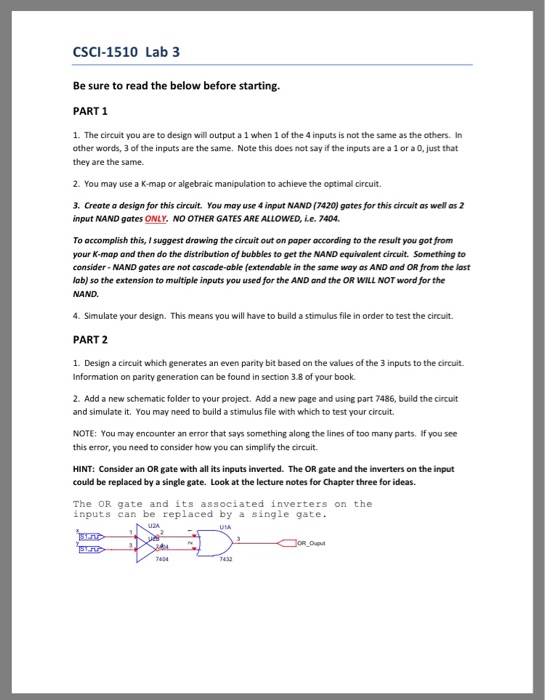
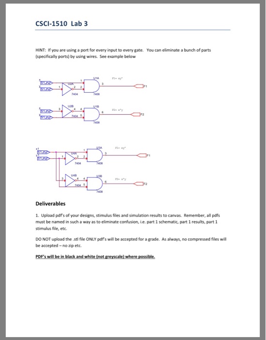
image text in transcribed
CSCI-1510 Lab 3 Be sure to read the below before starting. PART 1 1. The circuit you are to design will output a 1 when 1 of the 4 inputs is not the same as the others. In other words, 3 of the inputs are the same. Note this does not say if the inputs are a 1 or a 0, just that they are the same. 2. You may use a K-map or algebraic manipulation to achieve the optimal circuit 3. Create a design for this circuit. You may use 4 input NAND (7420) gates for this circuit as well as 2 nput NAND gates ONLY NO OTHER GATES ARE ALLOWED, ie. 7404 To accomplish this, I suggest drawing the circuit out on paper according to the result you got from your K-map and then do the distribution of bubbles to get the NAND equivalent circuit. Something to consider- NAND gates are not cascade-able (extendable in the same way as AND and OR from the last lab) so the extension to multiple inputs you used for the AND and the OR WILL NOT word for the NAND. 4. Simulate your design. This means you will have to build a stimulus file in order to test the circuit. PART 2 1. Design a circuit which generates an even parity bit based on the values of the 3 inputs to the circuit. Information on parity generation can be found in section 3.8 of your book. 2. Add a new schematic folder to your project. Add a new page and using part 7486, build the circuit and simulate it. You may need to build a stimulus file with which to test your circuit. NOTE: You may encounter an error that says something along the lines of too many parts. If you see this error, you need to consider how you can simplify the circuit HINT: Consider an OR gate with all its inputs inverted. The OR gate and the inverters on the input could be replaced by a single gate. Look at the lecture notes for Chapter three for ideas. The OR gate and its associated inverters on the inputs can be replaced by a single gate 404

Step by Step Solution

There are 3 Steps involved in it

Step: 1

blur-text-image

Get Instant Access to Expert-Tailored Solutions

See step-by-step solutions with expert insights and AI powered tools for academic success

Step: 2

blur-text-image

Step: 3

blur-text-image

Ace Your Homework with AI

Get the answers you need in no time with our AI-driven, step-by-step assistance

Get Started

Recommended Textbook for

DB2 9 For Linux UNIX And Windows Advanced Database Administration Certification Certification Study Guide

Authors: Roger E. Sanders, Dwaine R Snow

1st Edition

1583470808, 978-1583470800

More Books

Students also viewed these Databases questions