Question
Draw the logic diagram of the digit circuit specified by the following Verilog description: (a) module Circuit_A (A, B, C, D, F); input A, B,
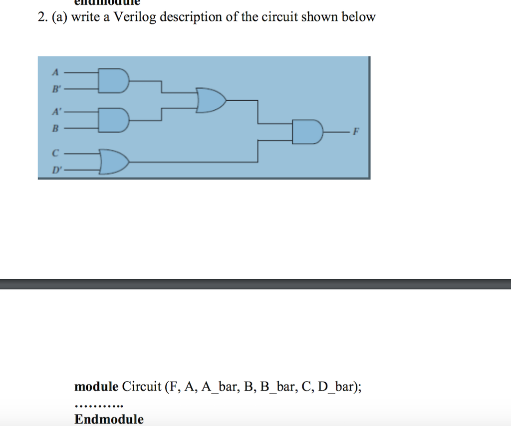
Draw the logic diagram of the digit circuit specified by the following Verilog description: (a) module Circuit_A (A, B, C, D, F); input A, B, C, D; output F; wire w, x, y, z, a, d; or (x, B, C, d); and (y, a ,C); and (w, z ,B); and (z, y, A); or (F, x, w); not (a, A); not (d, D); endmodule (b) module Circuit_B (y1, y2, y3, a, b); output y1, y2, y3; input a, b; assign y1 = a || b; and (y2, a, b); assign y3 = a && b; endmodule 2. (a) write a Verilog description of the circuit shown below
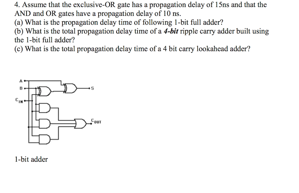
module Circuit (F, A, A_bar, B, B_bar, C, D_bar); ........... Endmodule (b) Write a Verilog description of the circuit specified by the following Boolean function: Z = (A + B)C(C + D) 3. The adder-subtractor has the following values for mode input M and data inputs A and B: M A B (a) 0 1100 1000 (b) 1 0111 0110 (c) 1 0000 0001 (d) 0 0101 1010 In each case, determine the values of the SUM outputs, the carry C, and overflow V. 4. Assume that the exclusive-OR gate has a propagation delay of 15ns and that the AND and OR gates have a propagation delay of 10 ns. (a) What is the propagation delay time of following 1-bit full adder? (b) What is the total propagation delay time of a 4-bit ripple carry adder built using the 1-bit full adder? (c) What is the total propagation delay time of a 4 bit carry lookahead adder?
1-bit adder
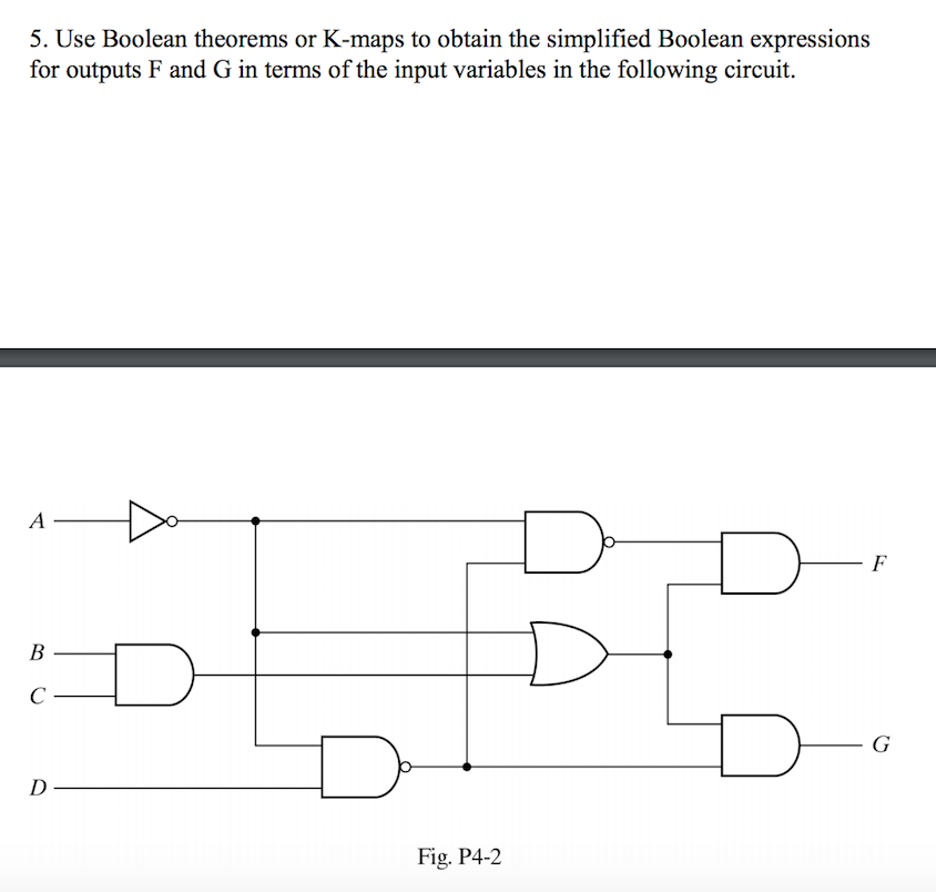
5. Use Boolean theorems or K-maps to obtain the simplified Boolean expressions for outputs F and G in terms of the input variables in the following circuit.
6. Use 4 half-adders to design a four-bit combinational circuit increamenter (a circuit that adds 1 to a four-bit binary number). Draw the logic diagram. 7. Draw the logic diagram of a combinational circuit that compares two four-bit numbers if they are equal. The circuit output is equal to 1 if the two numbers are equal and 0 otherwise. (hint: XOR or XNOR gate can be used to check if two bits are equal).
10 points each for the following questions. For the following circuit design questions, you must show the procedure of obtaining the truth-table, obtaining the simplified logic function using k-map, and drawing logic diagram. 8. (a) Design a half-subtractor circuit with inputs x and y and outputs Diff and Bout . The circuit subtracts the bits x y and places the difference in D and the borrow in Bout. (b) Design a full-subtractor circuit with three inputs x, y, Bin and two outputs Diff and Bout. The circuit subtracts x y Bin, where B in is the input borrow, Bout is the output


Step by Step Solution
There are 3 Steps involved in it
Step: 1

Get Instant Access to Expert-Tailored Solutions
See step-by-step solutions with expert insights and AI powered tools for academic success
Step: 2

Step: 3

Ace Your Homework with AI
Get the answers you need in no time with our AI-driven, step-by-step assistance
Get Started


