

Answered step by step
Verified Expert Solution
Question
1 Approved Answer
Edit: I'm not quite sure what needs to be added since all the comment said was no. 1. MOS Capacitor on n-type Si. Consider a
Edit: I'm not quite sure what needs to be added since all the comment said was "no."
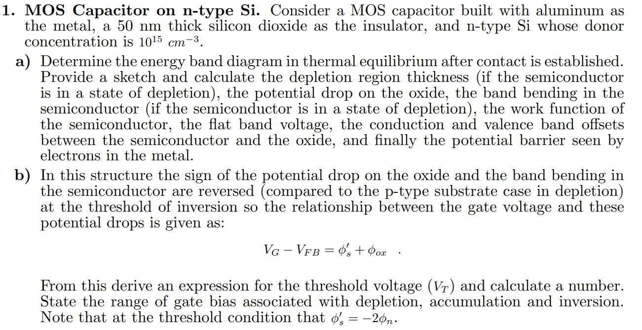
1. MOS Capacitor on n-type Si. Consider a MOS capacitor built with aluminum as the metal, a 50 nm thick silicon dioxide as the insulator, and n-type Si whose donor concentration is 1015 cm-3. a) Determine the energy band diagram in thermal equilibrium after contact is established. Provide a sketch and calculate the depletion region thickness (if the semiconductor is in a state of depletion), the potential drop on the oxide, the band bending in the semiconductor (if the semiconductor is in a state of depletion), the work function of the semiconductor, the flat band voltage, the conduction and valence band offsets between the semiconductor and the oxide, and finally the potential barrier seen by electrons in the metal. b) In this structure the sign of the potential drop on the oxide and the band bending in the semiconductor are reversed (compared to the p-type substrate case in depletion) at the threshold of inversion so the relationship between the gate voltage and these potential drops is given as: VG - VfB = ''s + Pox. From this derive an expression for the threshold voltage (VT) and calculate a number. State the range of gate bias associated with depletion, accumulation and inversion. Note that at the threshold condition that o' = -20n. 1. MOS Capacitor on n-type Si. Consider a MOS capacitor built with aluminum as the metal, a 50 nm thick silicon dioxide as the insulator, and n-type Si whose donor concentration is 1015 cm-3. a) Determine the energy band diagram in thermal equilibrium after contact is established. Provide a sketch and calculate the depletion region thickness (if the semiconductor is in a state of depletion), the potential drop on the oxide, the band bending in the semiconductor (if the semiconductor is in a state of depletion), the work function of the semiconductor, the flat band voltage, the conduction and valence band offsets between the semiconductor and the oxide, and finally the potential barrier seen by electrons in the metal. b) In this structure the sign of the potential drop on the oxide and the band bending in the semiconductor are reversed (compared to the p-type substrate case in depletion) at the threshold of inversion so the relationship between the gate voltage and these potential drops is given as: VG - VfB = ''s + Pox. From this derive an expression for the threshold voltage (VT) and calculate a number. State the range of gate bias associated with depletion, accumulation and inversion. Note that at the threshold condition that o' = -20nStep by Step Solution
There are 3 Steps involved in it
Step: 1

Get Instant Access to Expert-Tailored Solutions
See step-by-step solutions with expert insights and AI powered tools for academic success
Step: 2

Step: 3
Ace Your Homework with AI
Get the answers you need in no time with our AI-driven, step-by-step assistance
Get Started
Corporate Governance A Pragmatic Guide For Auditors Directors Investors And Accountants Internal Audit And IT Audit
Authors: Vasant Raval
1st Edition
0367862751, 978-0367862756