

Answered step by step
Verified Expert Solution
Question
1 Approved Answer
ELL201/ELP201: Digital Electronics Laboratory Lab Project Design a sequence generator that generates the following serial sequence: If your Entry no. is 2021EE1X1X2X3X4, then the
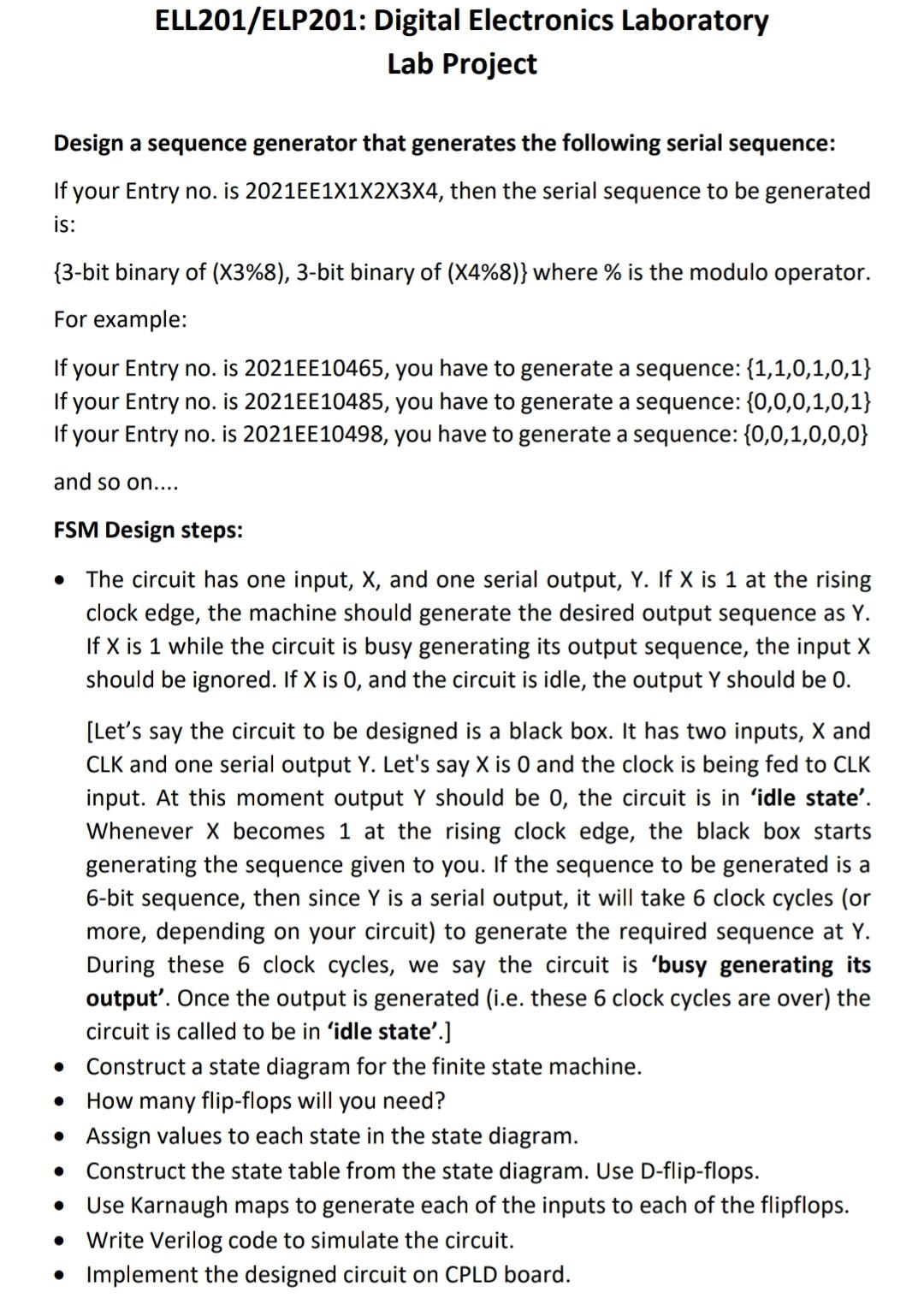
ELL201/ELP201: Digital Electronics Laboratory Lab Project Design a sequence generator that generates the following serial sequence: If your Entry no. is 2021EE1X1X2X3X4, then the serial sequence to be generated is: {3-bit binary of (X3%8), 3-bit binary of (X4%8)} where % is the modulo operator. For example: If your Entry no. is 2021EE10465, you have to generate a sequence: {1,1,0,1,0,1} If your Entry no. is 2021EE10485, you have to generate a sequence: {0,0,0,1,0,1} If your Entry no. is 2021EE10498, you have to generate a sequence: {0,0,1,0,0,0} and so on.... FSM Design steps: The circuit has one input, X, and one serial output, Y. If X is 1 at the rising clock edge, the machine should generate the desired output sequence as Y. If X is 1 while the circuit is busy generating its output sequence, the input X should be ignored. If X is 0, and the circuit is idle, the output Y should be 0. [Let's say the circuit to be designed is a black box. It has two inputs, X and CLK and one serial output Y. Let's say X is 0 and the clock is being fed to CLK input. At this moment output Y should be 0, the circuit is in 'idle state'. Whenever X becomes 1 at the rising clock edge, the black box starts generating the sequence given to you. If the sequence to be generated is a 6-bit sequence, then since Y is a serial output, it will take 6 clock cycles (or more, depending on your circuit) to generate the required sequence at Y. During these 6 clock cycles, we say the circuit is 'busy generating its output'. Once the output is generated (i.e. these 6 clock cycles are over) the circuit is called to be in 'idle state'.] Construct a state diagram for the finite state machine. How many flip-flops will you need? Assign values to each state in the state diagram. Construct the state table from the state diagram. Use D-flip-flops. Use Karnaugh maps to generate each of the inputs to each of the flipflops. Write Verilog code to simulate the circuit. Implement the designed circuit on CPLD board.
Step by Step Solution
There are 3 Steps involved in it
Step: 1

Get Instant Access to Expert-Tailored Solutions
See step-by-step solutions with expert insights and AI powered tools for academic success
Step: 2

Step: 3
Ace Your Homework with AI
Get the answers you need in no time with our AI-driven, step-by-step assistance
Get Started
Auditing An International Approach
Authors: Wally J. Smieliauskas, Kathryn Bewley
6th edition
978-0070968295, 9781259087462, 978-0071051415