

Question: Fig. 1 below shows a four-stage shift-register connected with exclusive-or gates to form a state machine exclusive-or clock Figure 1. Feedback Shift Register State Machine
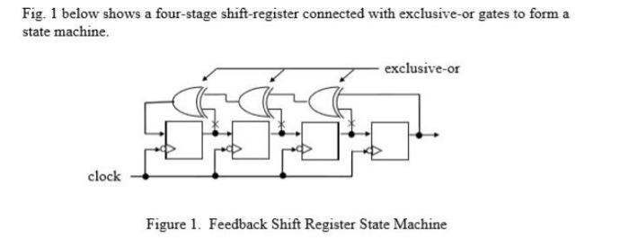

Fig. 1 below shows a four-stage shift-register connected with exclusive-or gates to form a state machine exclusive-or clock Figure 1. Feedback Shift Register State Machine 2. Pseudorandom Sequence Generator Step A below asks you to complete a paper design of the PSG as if you were going to implement it using discrete gates. It is important to complete this step, as it will add significantly to your understanding of how the PSG operates. Our actual implementation, however, will be in software running on a PIC microcontroller A. Determine a proper set of connections so that the feedback shift register shown in Fig. 1 wil generate a pseudorandom sequence. With only eight possibilities it is safe to design the circuit using a trial and error" approach. Start with one possible configuration and run the circuit through its state sequence, assuming the flip-flops start in some non-zero initial state. If your circuit is a valid PSG, all 15 possible non zero states will be visited before the sequence repeats. (This behavior must be verified on paper) If it is not valid, try another configuration (Note: There are two valid PSG configurations, either of which will do the job.) Record a valid circuit in your notebook The serial data sequence read from (any) one of the D flip-flop outputs is a pseudorandom data signal that can be used as the information source to test a communication system. Record the pseudorandom data signal in your lab notebook, both as a serial bitstream and as a unipolar NRZ waveform. Contrary to the customary default practice,we will want the pseudorandom sequence generator to be triggered on the falling clock edge to simplify the timing at the data receiver later on. Show the falling edge trigger on your schematic diagram. B. After completing Step A you are ready to implement the PSG on a PIC microcontroller. Examine the data sheet for the PIC 16F690 and answer the following questions in your lab notebook a. Locate the pin diagram for the PIC 16F690. How many pins does the device have? Which pin is Vp? Which pin is V pin? Which of these two is the ground b. The PIC 16F690 has three registers for digital IO, labeled "RA," "RB." and "RC." How many pins does each of these registers have? c. What is the pin number of RC0 RC1? What is the number of the interrupt pin? d. Section 17 of the data sheet contains the electrical specifications. What is the intended supply voltage? What is the absolute maximum voltage allowed between I'm and i's? C. The program for the PSG is written in assembly language and is available in the class folder. The program consists of an interrupt routine and a main program having an initialization sequence followed by an endless loop. (The loop begins after the comment This is the main loop.") The microcontroller PSG implementation uses a 16-bit shift register rather than a 4-bit register as in Step A above. Do the following: a. Determine the period of the entire pseudorandom sequence if the clock frequency is 100 Hz. (Hint How long is the sequence generated by a 16-bit shift register?) b. Extra credit: If you are adept at assembly language, examine the program and draw a schematic as you did in Step A, showing the feedback connections for the 16-bit PSG. The assembly language instructions are described in Section 15 of the data sheet
Step by Step Solution
There are 3 Steps involved in it

Get step-by-step solutions from verified subject matter experts