Answered step by step
Verified Expert Solution
Question
1 Approved Answer
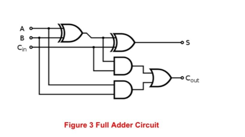
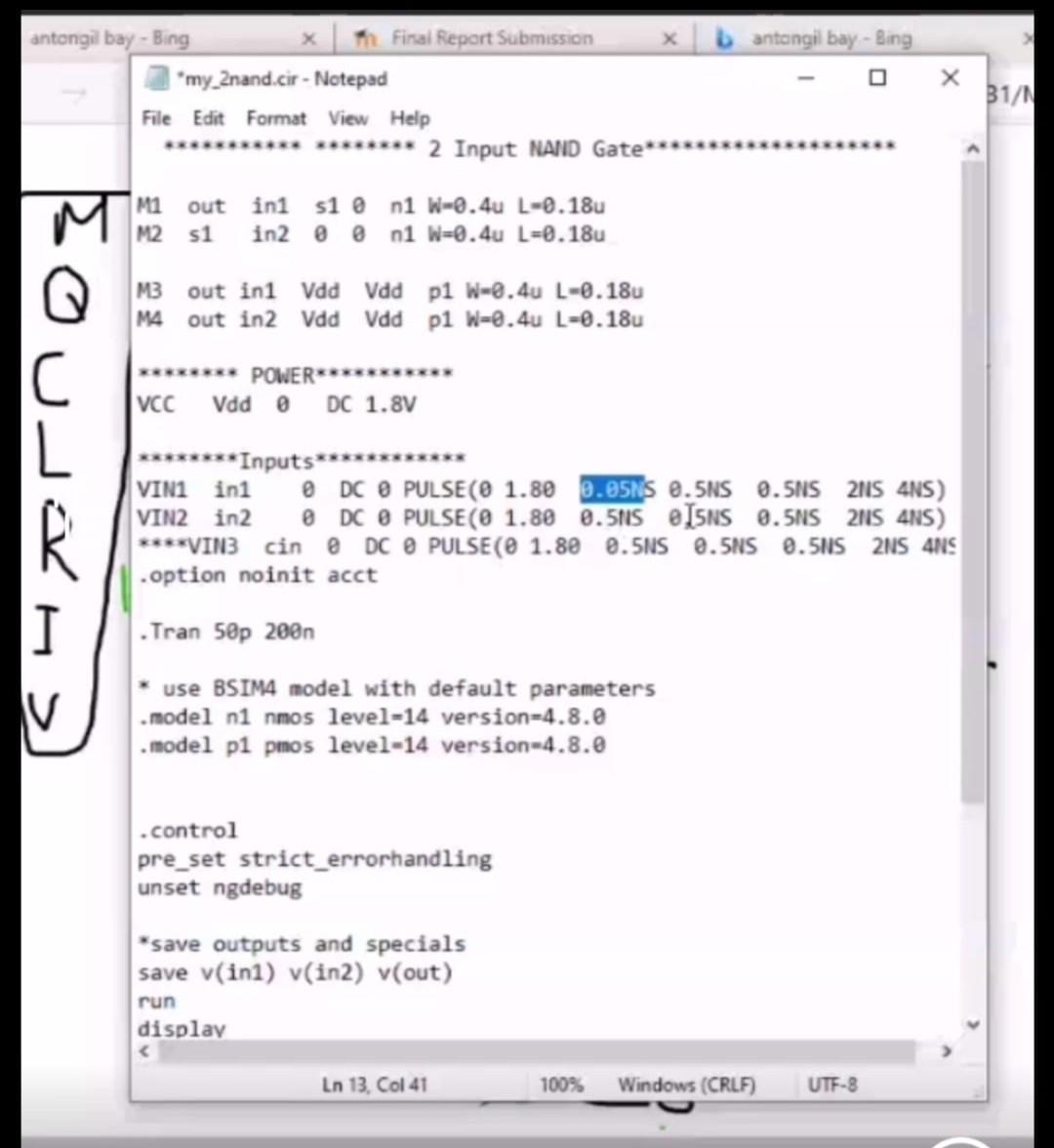
Figer 3 Figer 4 Electronics U need result of the circuit in figer 3,,by using NG SPACE Program. Same as showing in figer 4. The

Figer 3

Figer 4
Electronics U need result of the circuit in figer 3,,by using NG SPACE Program. Same as showing in figer 4. The result should be wave and Code same as show in figer 4.
D D os Cin Cout D Figure 3 Full Adder Circuit 31/1 antongil bay - Bing Final Report Submission xantongil bay - Bing *my_2nand.cir - Notepad File Edit Format View Help *********** ******** 2 Input NAND Gate**** out ini s1 e n1 W-0.4u L-0.18u M2 si in2 On1 W=0.4u L-0.18u M3 out ini Vdd Vdd p1 W-8.4u L-0.18u M4 out in2 Vad Vad p1 W=0.4u L-0.18u M so POWER*********** Vdd DC 1.8V VCC Q C L IR I ******Inputs******* VINI ini DC @ PULSE(O 1.89 0.85 0.5NS 0.5NS 2NS ANS) VIN2 in2 0 DC O PULSE (0 1.80 0.5NS I5NS 0.5NS 2NS ANS) ****VIN3 cin DC O PULSE(O 1.80 0.5 0.5 0.5NS 2NS 4NS .option noinit acct Iran 5p 200n. v use BSIM4 model with default parameters . model ni nmos level-14 version 4.8.0 . model pi pmos level-14 version 4.8.0 .control pre_set strict_errorhandling unset ngdebug "save outputs and specials save v(int) v(in2) v(out) run displayStep by Step Solution
There are 3 Steps involved in it
Step: 1

Get Instant Access to Expert-Tailored Solutions
See step-by-step solutions with expert insights and AI powered tools for academic success
Step: 2

Step: 3

Ace Your Homework with AI
Get the answers you need in no time with our AI-driven, step-by-step assistance
Get Started


