Question
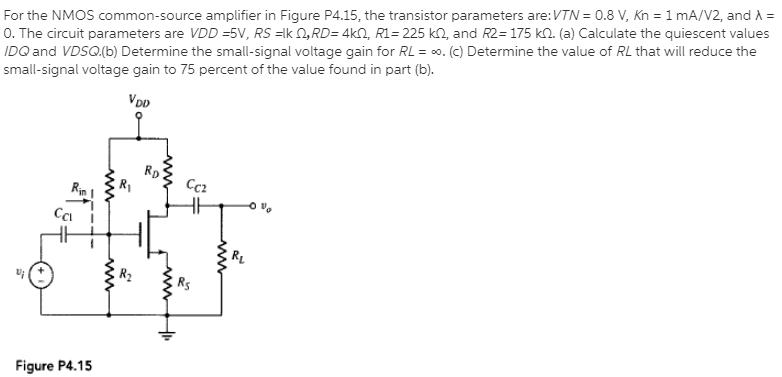
For the NMOS common-source amplifier in Figure P4.15, the transistor parameters are:VTN = 0.8 V, Kn = 1 mA/V2, and A = 0. The

For the NMOS common-source amplifier in Figure P4.15, the transistor parameters are:VTN = 0.8 V, Kn = 1 mA/V2, and A = 0. The circuit parameters are VDD =5V, RS =lk 0, RD= 4kN, R1= 225 kN, and R2=175 kn. (a) Calculate the quiescent values IDQ and VDSQ(b) Determine the small-signal voltage gain for RL = 0. (c) Determine the value of RL that will reduce the small-signal voltage gain to 75 percent of the value found in part (b). VDD Rp R1 Cc2 Rin RL Figure P4.15
Step by Step Solution
3.37 Rating (166 Votes )
There are 3 Steps involved in it
Step: 1

Get Instant Access to Expert-Tailored Solutions
See step-by-step solutions with expert insights and AI powered tools for academic success
Step: 2

Step: 3

Ace Your Homework with AI
Get the answers you need in no time with our AI-driven, step-by-step assistance
Get StartedRecommended Textbook for
Modern Control Systems
Authors: Richard C. Dorf, Robert H. Bishop
12th edition
136024580, 978-0136024583
Students also viewed these Electrical Engineering questions
Question
Answered: 1 week ago
Question
Answered: 1 week ago
Question
Answered: 1 week ago
Question
Answered: 1 week ago
Question
Answered: 1 week ago
Question
Answered: 1 week ago
Question
Answered: 1 week ago
Question
Answered: 1 week ago
Question
Answered: 1 week ago
Question
Answered: 1 week ago
Question
Answered: 1 week ago
Question
Answered: 1 week ago
Question
Answered: 1 week ago
Question
Answered: 1 week ago
Question
Answered: 1 week ago
Question
Answered: 1 week ago
Question
Answered: 1 week ago
Question
Answered: 1 week ago
Question
Answered: 1 week ago
Question
Answered: 1 week ago
Question
Answered: 1 week ago
View Answer in SolutionInn App


