Answered step by step
Verified Expert Solution
Question
1 Approved Answer
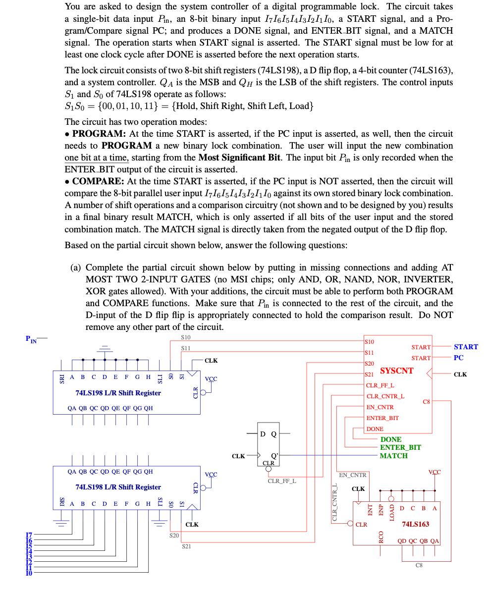
PIN You are asked to design the system controller of a digital programmable lock. The circuit takes a single-bit data input Pin, an 8-bit


PIN You are asked to design the system controller of a digital programmable lock. The circuit takes a single-bit data input Pin, an 8-bit binary input I7I6I5I4I3I2I1I0, a START signal, and a Pro- gram/Compare signal PC; and produces a DONE signal, and ENTER-BIT signal, and a MATCH signal. The operation starts when START signal is asserted. The START signal must be low for at least one clock cycle after DONE is asserted before the next operation starts. The lock circuit consists of two 8-bit shift registers (74LS198), a D flip flop, a 4-bit counter (74LS163), and a system controller. QA is the MSB and QH is the LSB of the shift registers. The control inputs S and So of 74LS198 operate as follows: S1 So 00, 01, 10, 11} = {Hold, Shift Right, Shift Left, Load} The circuit has two operation modes: PROGRAM: At the time START is asserted, if the PC input is asserted, as well, then the circuit needs to PROGRAM a new binary lock combination. The user will input the new combination one bit at a time, starting from the Most Significant Bit. The input bit Pin is only recorded when the ENTER BIT output of the circuit is asserted. COMPARE: At the time START is asserted, if the PC input is NOT asserted, then the circuit will compare the 8-bit parallel user input 1716151413121110 against its own stored binary lock combination. A number of shift operations and a comparison circuitry (not shown and to be designed by you) results in a final binary result MATCH, which is only asserted if all bits of the user input and the stored combination match. The MA CH signal is directly taken from the negated output of the flip flop. Based on the partial circuit shown below, answer the following questions: SRII (a) Complete the partial circuit shown below by putting in missing connections and adding AT MOST TWO 2-INPUT GATES (no MSI chips; only AND, OR, NAND, NOR, INVERTER, XOR gates allowed). With your additions, the circuit must be able to perform both PROGRAM and COMPARE functions. Make sure that Pin is connected to the rest of the circuit, and the D-input of the D flip flip is appropriately connected to hold the comparison result. Do NOT remove any other part of the circuit. $10 $11 A B DE F G H 74LS198 L/R Shift Register QA QB QC QD QE QF QG QH QA QB QC QD QE QF QG QH 74LS198 L/R Shift Register A B C D E F G H E $20 CLK S21 CLK VCC VCC CLK -D O Q' CLR O CLR FF L CLR_CNTR_L $10 $11 $20 S21 CLR FF L CLR CNTR_L EN CNTR ENTER_BIT DONE EN CNTR CLK CLR SYSCNT START START DONE ENTER BIT MATCH RCO LOAD C8 D C B VCC 74LS163 C8 A QD QC QB QA START PC CLK (b) Based on your response in Part (a), provide a state diagram for the System Controller (SYSCNT) with the format clearly shown. Do not complete other steps of the design process. Do not use more than eight states. Implement Moore-type outputs. Use a legend to indicate your format. Select and use meaningful state names.
Step by Step Solution
★★★★★
3.45 Rating (152 Votes )
There are 3 Steps involved in it
Step: 1
Here are the steps to complete the circuit a To connect Pin to the circuit I add an inverter on the ...
Get Instant Access to Expert-Tailored Solutions
See step-by-step solutions with expert insights and AI powered tools for academic success
Step: 2

Step: 3

Ace Your Homework with AI
Get the answers you need in no time with our AI-driven, step-by-step assistance
Get Started


