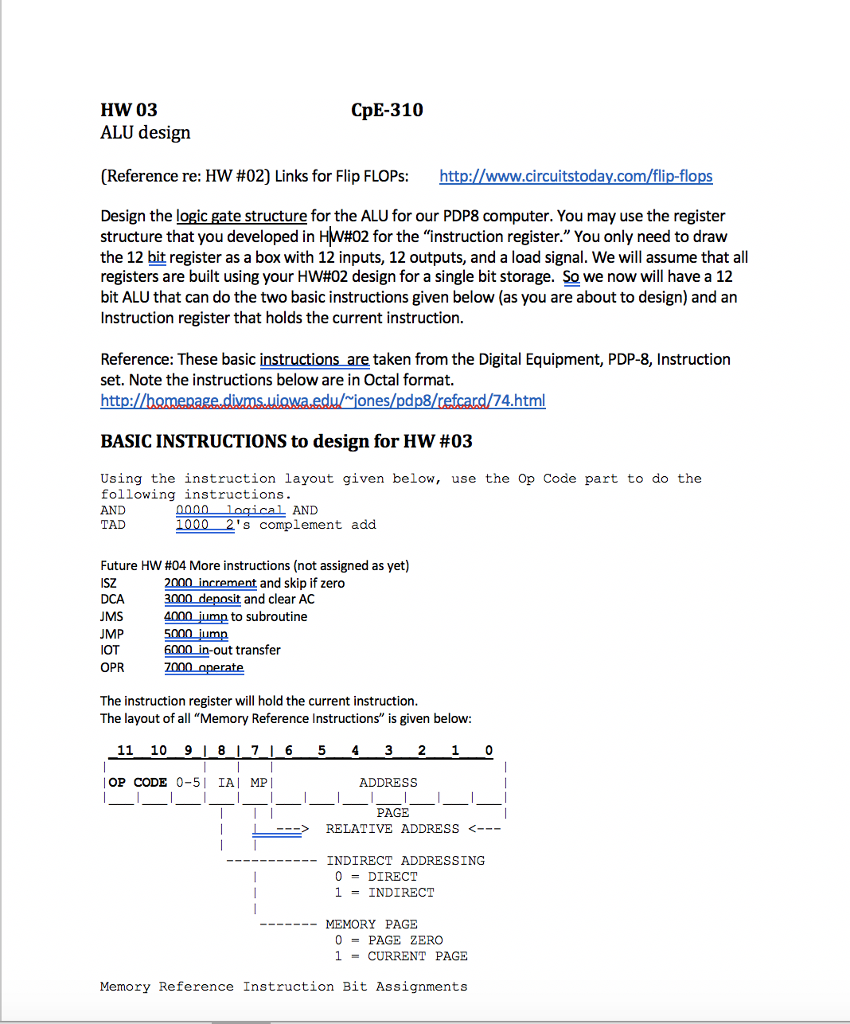
Question: HW 03 ALU design CpE-310 (Reference re: Hw #02) Links for Flip FLOPs: http://www.circuit today.com flip-flops Design the logic gate structure for the ALU for

HW 03 ALU design CpE-310 (Reference re: Hw #02) Links for Flip FLOPs: http://www.circuit today.com flip-flops Design the logic gate structure for the ALU for our PDP8 computer. You may use the register structure that you developed in HW#02 for the "instruction register." You only need to draw the 12 bit register as a box with 12 inputs, 12 outputs, and a load signal. We will assume that all registers are built using your HW#02 design for a single bit storage. So we now will have a 12 bit ALU that can do the two basic instructions given below (as you are about to design) and an Instruction register that holds the current instruction Reference: These basic instructions are taken from the Digital Equipment, PDP-8, Instruction set. Note the instructions below are in Octal format. ones 74 html BASIC INSTRUCTIONS to design for HW #03 Using the instruction layout given below, use the Op Code part to do the following instructions AND TAD AND 's complement add Future Hw #04 More instructions (not assigned as yet) JMS JMP OT OPR 2000 increment and skip if zero 3000 deposit and clear AC 4000 umn to subroutine 000 jump 6000 in-out transfer 2000 operate The instruction register will hold the current instruction The layout of all "Memory Reference Instructions" is given below: 11 10 987 6 5 3 2 0 OP CODE 0-5 IAI MPI ADDRESS PAGE > RELATIVE ADDRESS RELATIVE ADDRESS
Step by Step Solution
There are 3 Steps involved in it

Get step-by-step solutions from verified subject matter experts


