Answered step by step
Verified Expert Solution
Question
1 Approved Answer
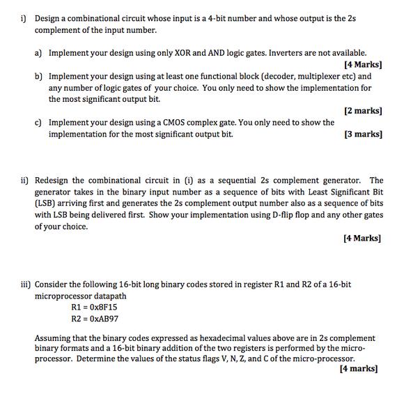
i) Design a combinational circuit whose input is a 4-bit number and whose output is the 2s complement of the input number. a) Implement


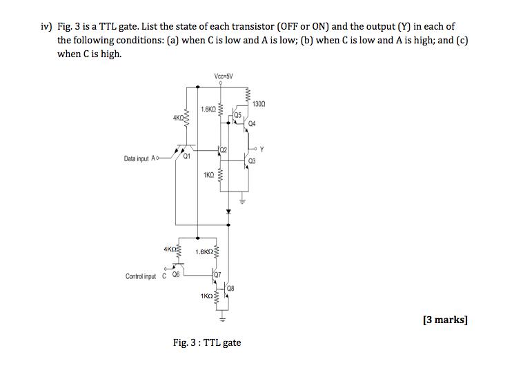
i) Design a combinational circuit whose input is a 4-bit number and whose output is the 2s complement of the input number. a) Implement your design using only XOR and AND logic gates. Inverters are not available. [4 Marks] b) Implement your design using at least one functional block (decoder, multiplexer etc) and any number of logic gates of your choice. You only need to show the implementation for the most significant output bit. [2 marks] [3 marks] c) Implement your design using a CMOS complex gate. You only need to show the implementation for the most significant output bit. ii) Redesign the combinational circuit in (i) as a sequential 2s complement generator. The generator takes in the binary input number as a sequence of bits with Least Significant Bit (LSB) arriving first and generates the 2s complement output number also as a sequence of bits with LSB being delivered first. Show your implementation using D-flip flop and any other gates of your choice. [4 Marks] iii) Consider the following 16-bit long binary codes stored in register R1 and R2 of a 16-bit microprocessor datapath R1 = 0x8F15 R2 = 0xAB97 Assuming that the binary codes expressed as hexadecimal values above are in 2s complement binary formats and a 16-bit binary addition of the two registers is performed by the micro- processor. Determine the values of the status flags V, N, Z, and C of the micro-processor. [4 marks] iv) Fig. 3 is a TTL gate. List the state of each transistor (OFF or ON) and the output (Y) in each of the following conditions: (a) when C is low and A is low; (b) when C is low and A is high; and (c) when C is high. Data input Ao- 4KQ- 4K02 Control input CQ6 01 1.6KQ 1KQ 1.6K Vcc=5V 1K2 www 02 Q7 05 Q8 Hi Fig. 3: TTL gate 1300 04 Q3 Y [3 marks]
Step by Step Solution
There are 3 Steps involved in it
Step: 1
The images reflect a series of digital electronics questions which include designing combinational circuits sequential circuits and analyzing the functionality of a TTL gate Here are the solutions to ...
Get Instant Access to Expert-Tailored Solutions
See step-by-step solutions with expert insights and AI powered tools for academic success
Step: 2

Step: 3

Ace Your Homework with AI
Get the answers you need in no time with our AI-driven, step-by-step assistance
Get Started


