I need help to fill out table 3 on page 88, and question 1 to 3 on page 89 to 90 Vo Monitor Run Monktor
I need help to fill out table 3 on page 88, and question 1 to 3 on page 89 to 90
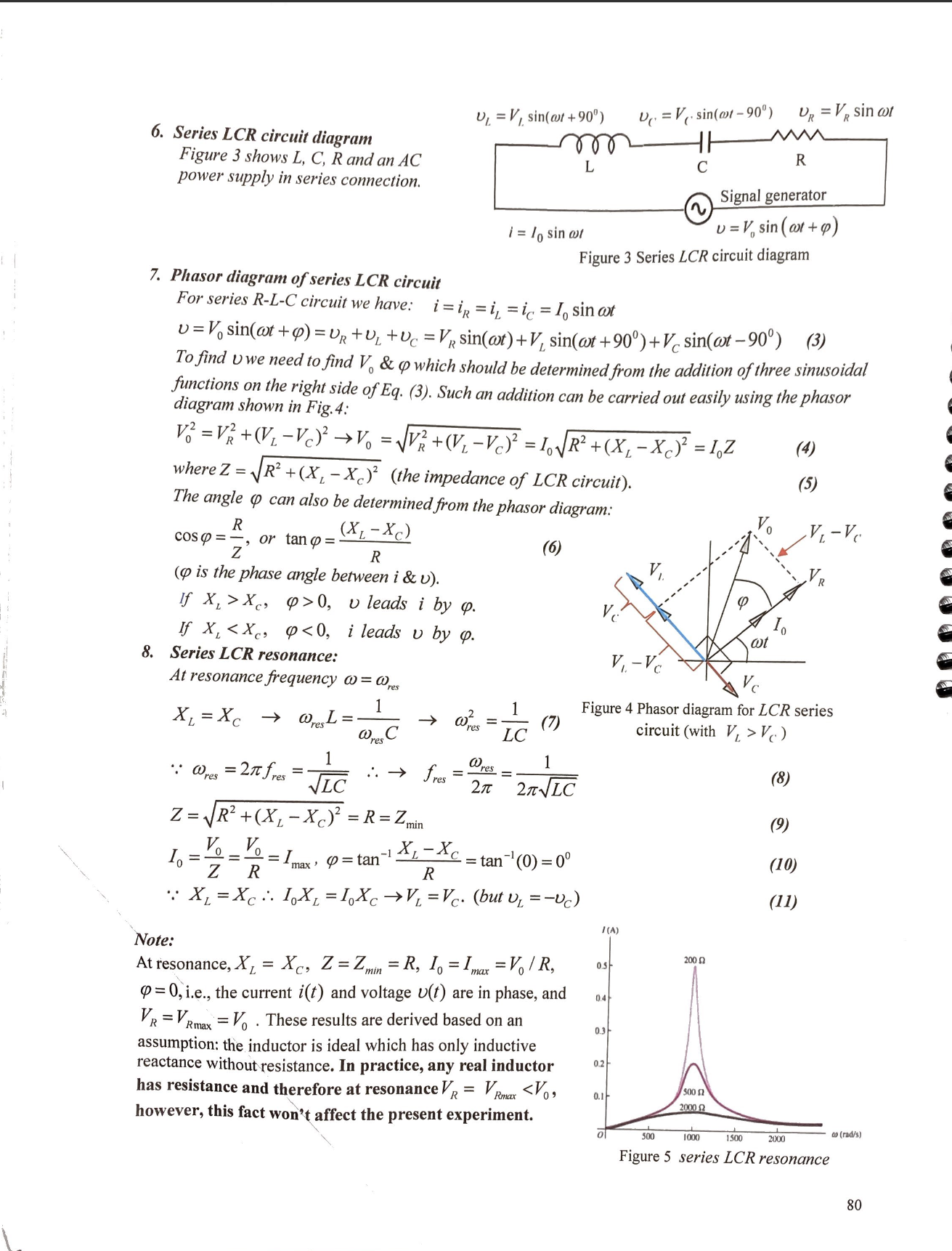
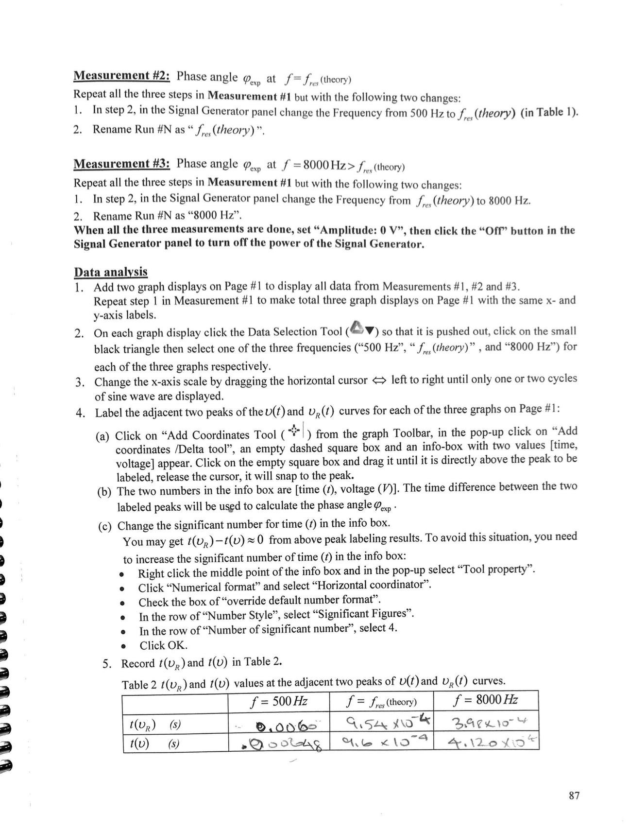
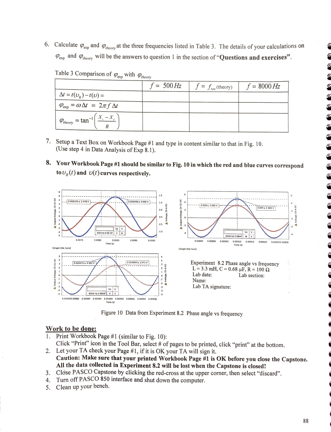
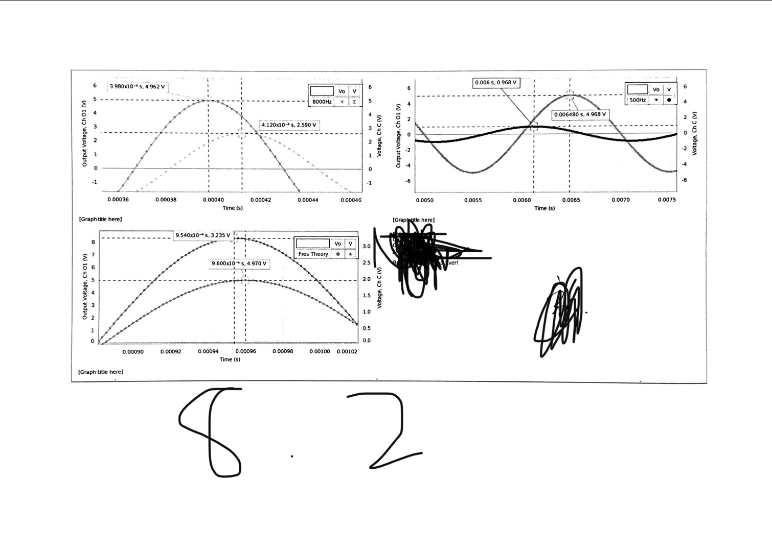
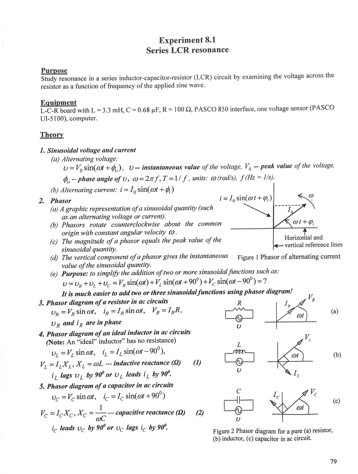
Vo Monitor Run Monktor Run Output Voltage, Ch 01 (v) Output Voltage, Ch 01 (v) IbWNNOHNWI -3 -2 - 1 1 0.0001 0.0002 0.0003 0.0004 0.0005 Voltage, Ch Ctv) Time (s) [Scope title here] [Graph title here] Monitor Run 2.5 3686.523 Hz, 1.571 V Squad Ever! " 2.0 Voltage, Ch C () 1.5 :-- 1.0 0.5 2000 4000 6000 8000 1000 0 Frequency (Hz) [FFT title here]6 3.980x10-" s. 4.962 V 0.006 s. 0.968 V Vo Vo V MIC 5 . 8000HZ 4 500Hz . A 0.006480 s. 4.968 v N 4.120x10-" s. 2.590 V AN ON A O O Voltage, Ch C (V) Output Voltage, Ch 01 (v) Output Voltage, Ch 01 (v) Voltage, Ch c (V) N JOHNWA N ab 0.00036 0.00038 0.00040 0.00042 0.00044 0.00046 0.0050 0.0055 0.0060 0.0065 0.0070 0.0075 Time (s) Time (s) [Graph title here] (Graph title here] 9.540x10-" s. 3.235 V- vo 3.0 Fres Theory 9.600x10* s. 4.970 V 2.5 ver 2.0 Output Voltage, Ch 01 (v) Voltage, Ch C (V 1.5 1.0 0.5 0.0 0.00090 0.00092 0.00094 0.00096 0.00098 0.00100 0.00102 Time (s) [ Graph title here] 6 2Experiment 8.1 Series LCR resonance Purpose Study resonance in a series inductor-capacitor-resistor (LCR) circuit by examining the voltage across the resistor as a function of frequency of the applied sine wave. Equipment L-C-R board with L = 3.3 mH, C =0.68 UF, R = 100 $, PASCO 850 interface, one voltage sensor (PASCO UI-5100), computer. Theory 1. Sinusoidal voltage and current (a) Alternating voltage: U= V. sin(@t + 8,), U-- instantaneous value of the voltage, Vo -- peak value of the voltage, do -- phase angle of U, @=2nf, T=1/ f , units: @ (rad/s), f (Hz = 1/s). (b) Alternating current: i = I, sin(wt + 4,) 2. Phasor i = 1, sin(wt+ 4,) w (a) A graphic representation of a sinusoidal quantity (such as an alternating voltage or current). (b) Phasors rotate counterclockwise about the common origin with constant angular velocity W. c) The magnitude of a phasor equals the peak value of the Horizontal and sinusoidal quantity. vertical reference lines 'd) The vertical component of a phasor gives the instantaneous Figure 1 Phasor of alternating current value of the sinusoidal quantity. e) Purpose: to simplify the addition of two or more sinusoidal functions such as: U = UR +U, + Uc = VR sin(wt) + V, sin(wt +90) + Vc sin(wt -90) = ? It is much easier to add two or three sinusoidal functions using phasor diagram! 3. Phasor diagram of a resistor in ac circuits VR R UR = VR sin ct, iR = IR sin cot, VR = IRR, (a) UR and iR are in phase 4. Phasor diagram of an ideal inductor in ac circuits (Note: An "ideal" inductor" has no resistance) L U1 = VL sin wt, iz = 1, sin(wt -90), (b) V1 = I,XL, XL = WL --- inductive reactance ($2) (1) iz lags UL by 90 or UL leads iz by 90%. 5. Phasor diagram of a capacitor in ac circuits UC = Vc sin wt, ic = Ic sin(wt +90) (c) Vc = IcXc, XC =- -- capacitive reactance ($2) (2) ic leads Uc by 90 or vc lags ic by 90%. Figure 2 Phasor diagram for a pure (a) resistor, (b) inductor, (c) capacitor in ac circuit. 79U1 = V, sin(cut +90') U . = V . sin(@t -90') UR = VR sin cl M 6. Series LCR circuit diagram Figure 3 shows L, C, R and an AC R L C power supply in series connection. Signal generator 1 = 10 sin of U = V. sin (wt + () Figure 3 Series LCR circuit diagram 7. Phasor diagram of series LCR circuit For series R-L-C circuit we have: i = ip = 1, = ic = I, sin wt U = V. sin(ct + Vo = VVB + (V - Vc)? = 10VR2 + ( X, - Xc)? = 1.Z (4 ) where Z = \\R' +(X, -Xc) (the impedance of LCR circuit). (5) The angle @ can also be determined from the phasor diagram: cos @ = -, or tang = - ( X 1 - XC) V -V (6) R (p is the phase angle between i & U). VR If X, > Xc, 420, u leads i by p. If X, Wres = 7 LC (7) W pes circuit (with V, > Vc ) .: Wres = 2nt fres =- .. > fres = = Wres = VLC 27VLC (8) Z = \\R2 + (X, - Xc)? = R=Zmin (9) To =Z R Vo = Vo = In , = tan-I AL- AC = tan-(0) =00 (10) R " X 1 = Xc :. I.X, = 1.Xc ->V. = Vc. (but U, =-vc) (11) I (A) Note: At resonance, X1 = Xc, Z = Zmin = R, I. = Imax = Vo IR, os 200 9 p=0, i.e., the current i(t) and voltage U(t) are in phase, and 04 VR = VRmax = Vo . These results are derived based on an 0.3 assumption: the inductor is ideal which has only inductive reactance without resistance. In practice, any real inductor has resistance and therefore at resonance VR = VRmax f {theory} Repeat all the three steps in Measurement #1 but with the following two changes. l. in step 2, in the Signal Generator panel change the Frequency from fraheary) to 8000 Hz. 2. Rename Run #N as \"8000 Hz". When all the three measurements are done, set \"Amplitude: 0 V\6. Calculate Pexp and theory at the three frequencies listed in Table 3. The details of your calculations on Pexp and theory will be the answers to question 1 in the section of "Questions and exercises". Table 3 Comparison of Pexp with theory f = 500 Hz f = fres (theory) f = 8000 Hz At = t(UR) -1(0) = Pexp = WAt = 2nf At Ptheory = tan- X, -X R 7. Setup a Text Box on Workbook Page #1 and type in content similar to that in Fig. 10. (Use step 4 in Data Analysis of Exp 8.1). B. Your Workbook Page #1 should be similar to Fig. 10 in which the red and blue curves correspond to UR (1) and U(t) curves respectively. 1.5 -0.008102 5. 0 978 V 0.008498 5. 4.930 V- 1.0 -D.009 5. 3.292 V 0.009 . 4 986 V A Voltage, CHA() A Output Voltage. Ch 01 (V) A voltage Cha() Output Voltage. Ch OL (V) 500 M2 0 68 mi 3940 Hz 0.same 0.0075 0.0080 0.0085 0.0090 0.0095 Time (s) D.00895 0.00900 0.00905 0.00910 0 00915 00920 0.009250 00930 Time (s) (Graph title here] [Graph title here) A 296 , $ 9106090 0 009894 5. 2.571 V Experiment 8.2 Phase angle vs frequency L = 3.3 mH, C = 0.68 HF, R = 100 02 A voltage. Ch AM) A Output Voltage, Chol (V) Lab date: Lab section: Name Lab TA signature: 8000 MZ 0.68md 1 7 0.009800.00982 0.00984 0 00985 0.00968 0.00990 0.00992 0.00994 0.00996 Time (al Figure 10 Data from Experiment 8.2 Phase angle vs frequency Work to be done: 1. Print Workbook Page #1 (similar to Fig. 10): Click "Print" icon in the Tool Bar, select # of pages to be printed, click "print" at the bottom. 2. Let your TA check your Page #1, if it is OK your TA will sign it. Caution: Make sure that your printed Workbook Page #1 is OK before you close the Capstone. All the data collected in Experiment 8.2 will be lost when the Capstone is closed! 3. Close PASCO Capstone by clicking the red-cross at the upper corner, then select "discard". 4. Turn off PASCO 850 interface and shut down the computer. 5. Clean up your bench. 88
Step by Step Solution
There are 3 Steps involved in it
Step: 1
Get Instant Access to Expert-Tailored Solutions
See step-by-step solutions with expert insights and AI powered tools for academic success
Step: 2
Step: 3
Ace Your Homework with AI
Get the answers you need in no time with our AI-driven, step-by-step assistance