

Question: I need the answer as soon as possible Part 1: Simple implementation of Load, Store, and Add instructions. Objectives: 1- Design control sequence for a
I need the answer as soon as possible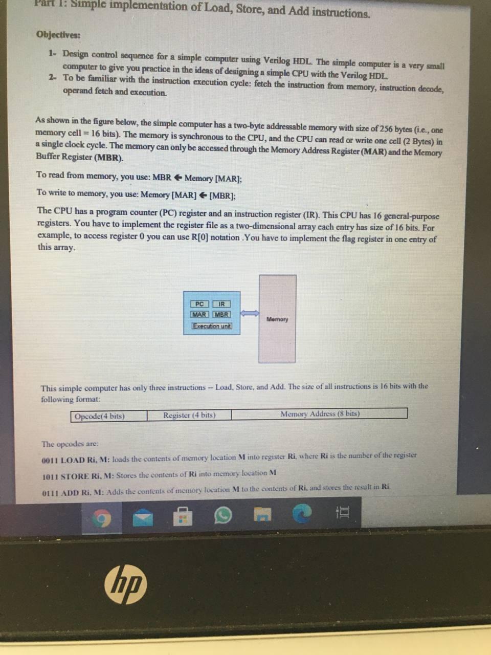
Part 1: Simple implementation of Load, Store, and Add instructions. Objectives: 1- Design control sequence for a simple computer using Verilog HDL. The simple computer is a very small computer to give you practice in the ideas of designing a simple CPU with the Verilog HDL. 2- To be familiar with the instruction execution cycle: fetch the instruction from memory, instruction decode, operand fetch and execution. As shown in the figure below, the simple computer has a two-byte addressable memory with size of 256 bytes (i.e., one memory cell = 16 bits). The memory is synchronous to the CPU, and the CPU can read or write one cell (2 Bytes) in a single clock cycle. The memory can only be accessed through the Memory Address Register (MAR) and the Memory Buffer Register (MBR). To read from memory, you use: MBR Memory [MAR]; To write to memory, you use: Memory [MAR] [MBR]; The CPU has a program counter (PC) register and an instruction register (IR). This CPU has 16 general-purpose registers. You have to implement the register file as a two-dimensional array each entry has size of 16 bits. For example, to access register 0 you can use R[0] notation. You have to implement the flag register in one entry of this array. PC IR MAR MBR Execution unk This simple computer has only three instructions - Load, Store, and Add. The size of all instructions is 16 bits with the following format: Opcode(4 bits) hp Memory Register (4 bits) Memory Address (8 bits) The opcodes are: 0011 LOAD Ri, M: loads the contents of memory location M into register Ri, where Ri is the number of the register 1011 STORE Ri, M: Stores the contents of Ri into memory location M 0111 ADD Ri. M: Adds the contents of memory location M to the contents of Ri, and stores the result in Ri
Step by Step Solution
3.43 Rating (162 Votes )
There are 3 Steps involved in it
Memory Address 20 21 22 30 31 32 Load RL 1307 Contents Load Rt 30 instruction ... View full answer

Get step-by-step solutions from verified subject matter experts