Answered step by step
Verified Expert Solution
Question
1 Approved Answer
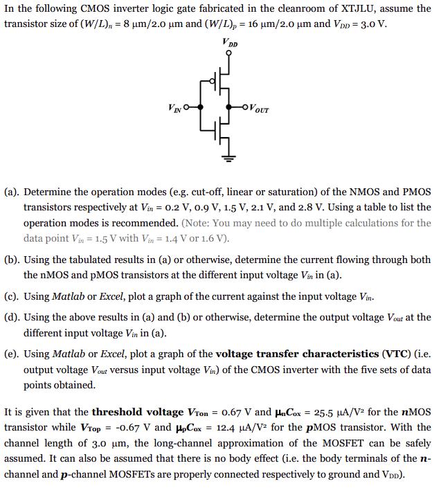
In the following CMOS inverter logic gate fabricated in the cleanroom of XTJLU, assume the transistor size of (W/L) = 8 m/2.0 m and

In the following CMOS inverter logic gate fabricated in the cleanroom of XTJLU, assume the transistor size of (W/L) = 8 m/2.0 m and (W/L), = 16 m/2.0 m and VDD = 3.0 V. V DD VIN -OVOUT (a). Determine the operation modes (e.g. cut-off, linear or saturation) of the NMOS and PMOS transistors respectively at Vin = 0.2 V, 0.9 V, 1.5 V, 2.1 V, and 2.8 V. Using a table to list the operation modes is recommended. (Note: You may need to do multiple calculations for the data point Vin = 1.5 V with Vin = 1.4 V or 1.6 V). (b). Using the tabulated results in (a) or otherwise, determine the current flowing through both the nMOS and PMOS transistors at the different input voltage Vin in (a). (c). Using Matlab or Excel, plot a graph of the current against the input voltage Vin. (d). Using the above results in (a) and (b) or otherwise, determine the output voltage Vout at the different input voltage Vin in (a). (e). Using Matlab or Excel, plot a graph of the voltage transfer characteristics (VTC) (i.e. output voltage Vout versus input voltage Vin) of the CMOS inverter with the five sets of data points obtained. It is given that the threshold voltage Vron = 0.67 V and nCox = 25.5 A/V for the nMOS transistor while VTop = -0.67 V and upCox = 12.4 A/V for the PMOS transistor. With the channel length of 3.0 um, the long-channel approximation of the MOSFET can be safely assumed. It can also be assumed that there is no body effect (i.e. the body terminals of the n- channel and p-channel MOSFETs are properly connected respectively to ground and VDD).
Step by Step Solution
★★★★★
3.41 Rating (154 Votes )
There are 3 Steps involved in it
Step: 1

Get Instant Access to Expert-Tailored Solutions
See step-by-step solutions with expert insights and AI powered tools for academic success
Step: 2

Step: 3

Ace Your Homework with AI
Get the answers you need in no time with our AI-driven, step-by-step assistance
Get Started


