Question: In this assignment, you are required to extend the MIPS-lite single-cycle implementation (discussed in your laboratory sessions) by implementing additional status register and instructions. You


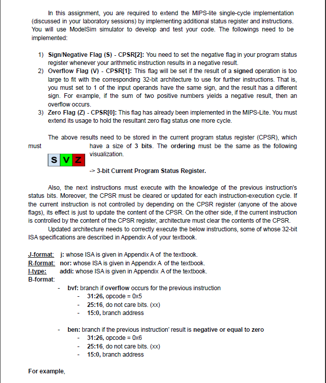
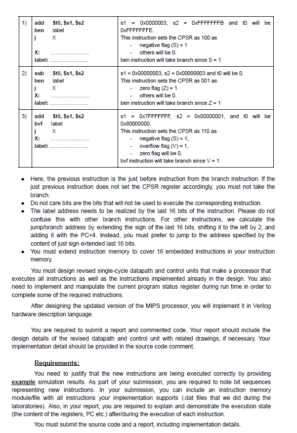
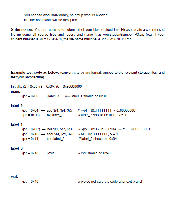
In this assignment, you are required to extend the MIPS-lite single-cycle implementation (discussed in your laboratory sessions) by implementing additional status register and instructions. You will use ModelSim simulator to develop and test your code. The followings need to be implemented: 1) Sign/Negative Flag (S) - CPSR[2]: You need to set the negative flag in your program status register whenever your arithmetic instruction results in a negative result. 2) Overflow Flag (V) - CPSR[1]: This flag will be set if the result of a signed operation is too large to fit with the corresponding 32-bit architecture to use for further instructions. That is, you must set to 1 of the input operands have the same sign, and the result has a different sign. For example, if the sum of two positive numbers yields a negative result, then an overflow occurs. 3) Zero Flag (Z) - CPSR[0]: This flag has already been implemented in the MIPS-Lite. You must extend its usage to hold the resultant zero flag status one more cycle. The above results need to be stored in the current program status register (CPSR), which must have a size of 3 bits. The ordering must be the same as the following visualization. 3-bit Current Program Status Register. Also, the next instructions must execute with the knowledge of the previous instruction's status bits. Moreover, the CPSR must be cleared or updated for each instruction-execution cycle. If the current instruction is not controlled by depending on the CPSR register (anyone of the above flags), its effect is just to update the content of the CPSR. On the other side, if the current instruction is controlled by the content of the CPSR register, architecture must clear the contents of the CPSR. Updated architecture needs to correctly execute the below instructions, some of whose 32-bit ISA specifications are described in Appendix A of your textbook. J-format: j : whose ISA is given in Appendix A of the textbook. R-format: nor: whose ISA is given in Appendix A of the textbook. l-type: addi: whose ISA is given in Appendix A of the textbook. B-format: - bvf: branch if overflow occurs for the previous instruction - 31:26, opcode =05 - 25:16, do not care bits. ( xx) - 15:0, branch address - ben: branch if the previous instruction' result is negative or equal to zero - 31:26, opcode =0x6 - 25:16, do not care bits. (xx) - 15:0, branch address For example, - Here, the previous instruction is the just before instruction from the branch instruction. If the just previous instruction does not set the CPSR register accordingly, you must not take the branch. - Do not care bits are the bits that will not be used to execute the corresponding instruction. - The label address needs to be realized by the last 16 bits of the instruction. Please do not confuse this with other branch instructions. For other instructions, we calculate the jump/branch address by extending the sign of the last 16 bits, shifting it to the left by 2 , and adding it with the PC+4. Instead, you must prefer to jump to the address specified by the content of just sign extended last 16 bits. - You must extend instruction memory to cover 16 embedded instructions in your instruction memory. You must design revised single-cycle datapath and control units that make a processor that executes all instructions as well as the instructions implemented already in the design. You also need to implement and manipulate the current program status register during run time in order to complete some of the required instructions. After designing the updated version of the MIPS processor, you will implement it in Verilog hardware description language. You are required to submit a report and commented code. Your report should include the design details of the revised datapath and control unit with related drawings, if necessary. Your implementation detail should be provided in the source code comment. Requirements: You need to justify that the new instructions are being executed correctly by providing example simulation results. As part of your submission, you are required to note bit sequences representing new instructions. In your submission, you can include an instruction memory module/file with all instructions your implementation supports (.dat files that we did during the laboratories). Also, in your report, you are required to explain and demonstrate the execution state (the content of the registers, PC etc.) after/during the execution of each instruction. You must submit the source code and a report, including implementation details. You need to work individually, no group work is allowed. No late homework will be accepted. Submission: You are required to submit all of your files to cloud-Ims. Please create a compressed file including all source files and report, and name it as yourstudentnumber_P3.zip (e.g. If your student number is 202112345678 , the file name must be 202112345678_P3.zip). Example test code as below: (convert it to binary format, embed to the relevant storage files, and test your architecture) Initially, 2=005,r3=00A,r5=080000000 main: \[ (\mathrm{pc}=0 \times 00) \text { - j label_1 } / / ightarrow \text { label_1 should be 0x0C } \] label_2: \[ \begin{array}{ll} (\mathrm{pc}=0 \times 04)-\text { add } \$ \mathrm{r} 4, \$ \mathrm{Sr} 4, \$ \mathrm{r} 5 & / / ightarrow \mathrm{r} 4=(0 \mathrm{xFFFFFFFF}+0 \times 80000000) \\ (\mathrm{pc}=0 \times 08)-\text { bvf label_3 } & / / \text { label_3 should be } 0 \times 18, \mathrm{~V}=1 \end{array} \] label_1: \[ \begin{array}{ll} (\mathrm{pc}=0 \times 0 \mathrm{C})-\text { nor } \$ \mathrm{r} 1, \$ \mathrm{r} 2, \$ \mathrm{r} 3 & / / \sim(\mathrm{r} 2=0 \times 05 \mid \mathrm{r} 3=0 \times 0 \mathrm{~A}) ightarrow \mathrm{r} 1=0 \times \mathrm{exFFFFFF0} \\ (\mathrm{pc}=0 \times 10)-\text { addi } \$ \mathrm{r} 4, \$ \mathrm{r} 1,0 \times 0 \mathrm{~F} & / / \mathrm{r} 4=0 \times \mathrm{OFFFFFFF}, \mathbf{S}=1 \\ (\mathrm{pc}=0 \times 14) \text { - ben label_2 } & / / \text { label_2 should be 0x04 } \end{array} \] label_3: (pc=018)jexit//exitshouldbe040 exit: (pc=040) // we do not care the code after exit branch
Step by Step Solution
There are 3 Steps involved in it

Get step-by-step solutions from verified subject matter experts


