Question: In this lab, you will obtain experience with sequential logic design, and study digital design using the Xilinx design package for FPGAs. It is assumed


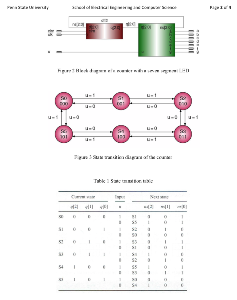
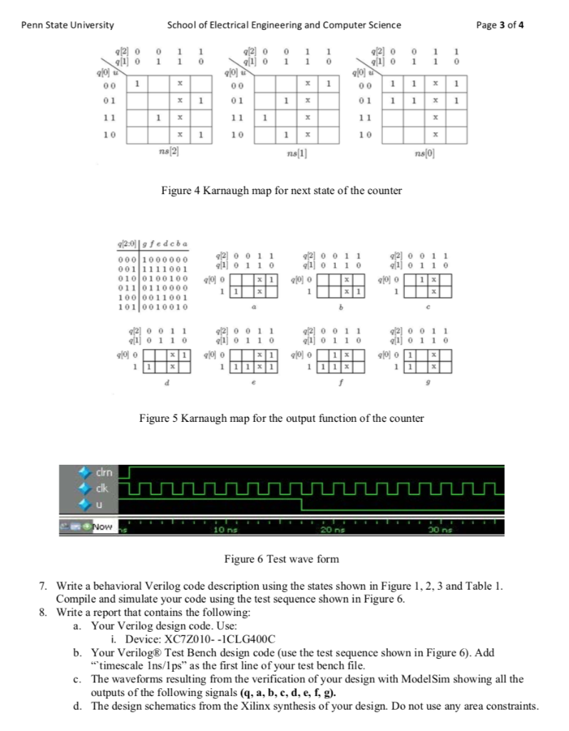
In this lab, you will obtain experience with sequential logic design, and study digital design using the Xilinx design package for FPGAs. It is assumed that the students are familiar with the operation of the Xilinx design package for Field Programmable Gate Arrays (FPGAs) through the Xilinix tutorial available in the class website 1. A finite state machine is a way of modeling system in which the system's output will depend on not only the current inputs but also the past history of inputs. It defines a finite set of states and behaviors, and how the system transits from one state to another when certain conditions are true. The module of output function is a combinational circuit that generates the outputs based on the current state (Moore model) or the combination of the current state and the current inputs (Mealy model) 2. Suppose we design a radix of six up/down counters as shown in Figure 1. The state of the counter changes on the positive (rising) edge of the clock. If the input u is a 1, the counter value will change in the sequence 0, 1, 2, 3, 4, 5, 0, 1,2, . If u is a 0, the counter value will change in the sequence 0, 5, 4, 3, 2, 1, 0, 5, 4, . There are seven output signals, with each connecting to a segment of LED. A segment of the LED will be on if its control signal is a 0 (active-low) There are six states, the circuit of the counter is shown in Figure 2. The module of dff3 contains three DFFs. The other module is a combinational circuit that generates signals of the next state (ns[2:0] and LED control signals (a, b, c, d, e, f, and g). The current state (the outputs of dff3) is denoted with q[2:0] Figure 3 shows the state transition diagram. The arrowed lines indicate the transitions of the states under the condition of the input. Figure 3 also shows that a 3-bit unique code is assigned to a state. Any code can be assigned to any state as long as all the codes are unique Table 1 is the truth table for the next state For students who took this class as an (honor option). Figure 4 shows the Karnaugh maps for each of the next state signals. From the Karnaugh maps, you can get the expressions of the next state signals. Figure 5 shows the truth table and Karnaugh maps of the output signals. You can get the expressions of the output signals from the Karnaugh maps 3. 4. 5. 6. drn Figure 1 A counter with a seven-segment LED Penn State University School of Electrical Engineering and Computer Science Page 2 of 4 q[20] 2020 nsl2 0 Figure 2 Block diagram of a counter with a seven segment LED S1 001 S2 010 u=0 u-0 u=1 | | u=0 u- 0 101 100 011 Figure 3 State transition diagram of the counter Table 1 State transition table Current state Input Next state ns2 s ns[0] SO0 1 S 0 0 S5 S 0 S2 0 S30 S2 0 0 SO0 S30 0 0 S 0 1 S4 0 S2 0 0 S4 I S5 0 S30 S5 SO0 S4 0 Penn State University School of Electrical Engineering and Computer Science Page 3 of 4 2 0 0 1 l 0 1 1 0 2] 0 01 1 1 1 0 0011 00 x1 01 1 1x1 0 1 0 1 1 0 1 0 ns 1 ns ns Figure 4 Karnaugh map for next state of the counter 000 1 000000 l 01 10 0 01010100100 011 0110000 100 0011001 101 0010010 01 1 0 l 0 1 0 1 01 1 0 l 01 10 Figure 5 Karnaugh map for the output function of the counter clrn clk 10 ns 20 ns 30ns Figure 6 Test wave form 7. Write a behavioral Verilog code description using the states shown in Figure 1,2, 3 and Table l Compile and simulate your code using the test sequence shown in Figure 6. Write a report that contains the following 8. a. Your Verilog design code. Use: i. Device: XC7Z010--1CLG400C b. Your VerilogR Test Bench design code (use the test sequence shown in Figure 6). Add timescale Ins/1ps" as the first line of your test bench file The waveforms resulting from the verification of your design with ModelSim showing all the outputs of the following signals (q, a, b, c, d, e, f, g). The design schematics from the Xilinx synthesis of your design. Do not use any area constraints c. d. In this lab, you will obtain experience with sequential logic design, and study digital design using the Xilinx design package for FPGAs. It is assumed that the students are familiar with the operation of the Xilinx design package for Field Programmable Gate Arrays (FPGAs) through the Xilinix tutorial available in the class website 1. A finite state machine is a way of modeling system in which the system's output will depend on not only the current inputs but also the past history of inputs. It defines a finite set of states and behaviors, and how the system transits from one state to another when certain conditions are true. The module of output function is a combinational circuit that generates the outputs based on the current state (Moore model) or the combination of the current state and the current inputs (Mealy model) 2. Suppose we design a radix of six up/down counters as shown in Figure 1. The state of the counter changes on the positive (rising) edge of the clock. If the input u is a 1, the counter value will change in the sequence 0, 1, 2, 3, 4, 5, 0, 1,2, . If u is a 0, the counter value will change in the sequence 0, 5, 4, 3, 2, 1, 0, 5, 4, . There are seven output signals, with each connecting to a segment of LED. A segment of the LED will be on if its control signal is a 0 (active-low) There are six states, the circuit of the counter is shown in Figure 2. The module of dff3 contains three DFFs. The other module is a combinational circuit that generates signals of the next state (ns[2:0] and LED control signals (a, b, c, d, e, f, and g). The current state (the outputs of dff3) is denoted with q[2:0] Figure 3 shows the state transition diagram. The arrowed lines indicate the transitions of the states under the condition of the input. Figure 3 also shows that a 3-bit unique code is assigned to a state. Any code can be assigned to any state as long as all the codes are unique Table 1 is the truth table for the next state For students who took this class as an (honor option). Figure 4 shows the Karnaugh maps for each of the next state signals. From the Karnaugh maps, you can get the expressions of the next state signals. Figure 5 shows the truth table and Karnaugh maps of the output signals. You can get the expressions of the output signals from the Karnaugh maps 3. 4. 5. 6. drn Figure 1 A counter with a seven-segment LED Penn State University School of Electrical Engineering and Computer Science Page 2 of 4 q[20] 2020 nsl2 0 Figure 2 Block diagram of a counter with a seven segment LED S1 001 S2 010 u=0 u-0 u=1 | | u=0 u- 0 101 100 011 Figure 3 State transition diagram of the counter Table 1 State transition table Current state Input Next state ns2 s ns[0] SO0 1 S 0 0 S5 S 0 S2 0 S30 S2 0 0 SO0 S30 0 0 S 0 1 S4 0 S2 0 0 S4 I S5 0 S30 S5 SO0 S4 0 Penn State University School of Electrical Engineering and Computer Science Page 3 of 4 2 0 0 1 l 0 1 1 0 2] 0 01 1 1 1 0 0011 00 x1 01 1 1x1 0 1 0 1 1 0 1 0 ns 1 ns ns Figure 4 Karnaugh map for next state of the counter 000 1 000000 l 01 10 0 01010100100 011 0110000 100 0011001 101 0010010 01 1 0 l 0 1 0 1 01 1 0 l 01 10 Figure 5 Karnaugh map for the output function of the counter clrn clk 10 ns 20 ns 30ns Figure 6 Test wave form 7. Write a behavioral Verilog code description using the states shown in Figure 1,2, 3 and Table l Compile and simulate your code using the test sequence shown in Figure 6. Write a report that contains the following 8. a. Your Verilog design code. Use: i. Device: XC7Z010--1CLG400C b. Your VerilogR Test Bench design code (use the test sequence shown in Figure 6). Add timescale Ins/1ps" as the first line of your test bench file The waveforms resulting from the verification of your design with ModelSim showing all the outputs of the following signals (q, a, b, c, d, e, f, g). The design schematics from the Xilinx synthesis of your design. Do not use any area constraints c. d
Step by Step Solution
There are 3 Steps involved in it

Get step-by-step solutions from verified subject matter experts


